At Mentor’s U2U this afternoon I attended a presentation on TSMC’s use of Calibre PERC (it is a programmable electrical rule checker) for qualification of IP in TSMC’s IP9000 program. I’ve written about this before here. Basically IP providers at N20SOC, N16FF, and below are required to use PERC to guarantee… Read More

Tag: finfet
FD-SOI, FinFET, 3D in Monterey
Last night the IEEE Silicon Valley Chapter had a panel session that was in some ways a preview of some of what will be discussed at the Electronic Design Process Symposium in Monterey next Thursday and Friday. At EDPS Herb Reiter organized a session on FinFET, 3DIC and FD-SOI (sort of how many buzzwords can you get into one set of titles).… Read More
SEMulator3D 2014 – New Enhancements for Virtual Fabrication in the 3D IC Era
A Virtual Platform for any kind of design or manufacturing in any discipline of science or engineering (electrical, mechanical, aeronautics etc.) must be able to provide an accurate representation of an actual design/product in a fraction of time and cost it takes to build working prototypes. In the case of semiconductors at … Read More
FinFET Custom Design
At CDNLive, Bob Mullen of TSMC gave a presentation on their new custom FinFET flow, doing design, and verifying designs. At 16nm there are all sorts of relatively new verification problems such as layout dependent effects (LDE) and voltage dependent design rules. We had some of this at 20nm but like most things in semiconductor,… Read More
IP Challenges, FinFET, 3D-IC, and FD-SOI Updates
Semiwiki is proud to be a sponsor of EDPS 2014:
April 17 & 18, 2014
Monterey Beach Hotel, Monterey, CA
Sponsored by:
IEEE Computer Society of Silicon Valley (CS-SCV)
IEEE Computer Society
Design Automation Technical Committee (DATC)
Council on Electronic Design Automation (CEDA)
The Electronic Design Processes Symposium… Read More
Handel Jones on FD-SOI vs FinFET
Handel Jones has a new white-paper out titled Why Migration to FD-SOI is a Better Approach Than Bulk CMOS and FinFETs at 20nm and 14/16nm for Price-Sensitive Markets. Handel has done an in-depth analysis of the wafer and die costs of the various approaches, bulk planar (what we have been doing up to now), FD-SOI and FinFET. The analysis… Read More
ISSCC: Analog-Digital Converter in FD-SOI
The International Solid-State Circuits Conference (ISSCC) was last week in San Francisco. Stéphane Le Tual, Pratap Narayan Singh, Christophe Curis, Pierre Dautriche, all from STMicroelectronics presented a paper on A 20GHz-BW 6b 10GS/s 32mW Time-Interleaved SAR ADC with Master T&H in 28nm UTBB FDSOI Technology… Read More
Designing an SoC with 16nm FinFET
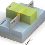
IC designers contemplating the transition to 16nm FinFET technology for their next SoC need to be informed about design flow and IP changes, so TSMC teamed up with Cadence Design Systems today to present a webinar on that topic. I attended the webinar and will summarize my findings.
Shown below is a 3D layout concept of an ideal FinFET… Read More
SOI Future or Flop?
Silicon On Insulator (SOI) is a technology that has been in use by the semiconductor industry for a long time. Early technologies such as Silicon On Sapphire (SOS) were reported as early as the sixties. In the eighties technologies such as V groove dielectric isolation were used. In the nineties we saw wafer bonding become the most… Read More
Why SOI is the Future Technology of Semiconductor
No doubt that FDSOI generate high interest these days and I found a very interesting contribution from Zvi Or-Bach, President and CEO of MonolithIC 3D, Inc. Zvi has accepted to share his wrap-up from IEDM, in a blog for Semiwiki readers. If you remember the long discussion we had in Semiwiki about cost comparison, some comments were… Read More