You are currently viewing SemiWiki as a guest which gives you limited access to the site. To view blog comments and experience other SemiWiki features you must be a registered member. Registration is fast, simple, and absolutely free so please,
join our community today!
Traditional logic testing relies on blasting pattern after pattern at the inputs, trying to exercise combinations to shake faults out of logic and hopefully have them manifested at an observable pin, be it a test point or a final output stage. It’s a remarkably inefficient process with a lot of randomness and luck involved.
Getting… Read More
As I see the semiconductor industry going through significant changes and advances, yet ironically plagued by a growing perception that the pace of scaling is slowing, I was inclined to take a peek into what the industry experts say about the state of the industry and the future of Moore’s Law. Fortunately, at last week’s International… Read More
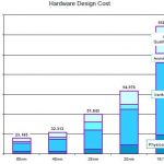
We agree now that FD-SOI technology is Faster, Cooler, Simpler. But can it also be a cheaper technology? Let start with an overview of the current estimation of the development cost for complex SoC on advanced technology nodes. The following data are extracted from International Business Strategies, Inc 2013 report. The first… Read More
One of the hottest areas for Application Specific Integrated Circuits today is Bitcoin mining. A good friend of mine has a son who is involved in a Bitcoin start-up so we have been discussing this at great length and I will share what I have learned thus far. Coincidently, my wife asked me about Bitcoin during our most recent walk down… Read More
I am at ARM TechCon today. One interesting presentation was made jointly between Samsung, Cadence and ARM themselves about developing physical libraries (ARM), a tool flow (Cadence) and test chips (Samsung). It was titled Samsung ARM and Cadence collaborate on the silicon-proven world first 14-nm FinFET Cortex-A7 ARM CPU and… Read More
Everywhere you turn these days you find FinFETs. Intel has had them since 22nm (they use the word Tri-gate but it is the same as what the world calls FinFET) and TSMC will have them at 16nm. So why FinFET? And is there an alternative?
The reason that regular bulk planar transistors have run out of steam is that the channel area underneath… Read More
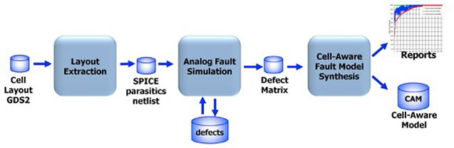
It’s a fact that new process nodes come with some amount of yield challenges. One way to find and eliminate silicon defects is through diagnosis-driven yield analysis (DDYA), which is the topic of a free seminar by Mentor Graphics in Fremont this Thursday, October 10 from 11:30am – 2pm (yes, lunch is included because Mentor… Read More
It is beginning to look as if 28nm transistors, which are the cheapest per million gates compared to any earlier process such as 45nm, may also be the cheapest per million gates compared to any later process such as 20nm.
What we know so far: FinFET seems to be difficult technology because of the 3D structure and so the novel manufacturing… Read More
Today TSMC announced three reference flows that they have been working on along with various EDA vendors (and ARM and perhaps other IP suppliers). The three new flows are:
- 16FinFET Digital Reference Flow. Obviously this has full support for non-planar FinFET transistors including extraction, quantized pitch placement, low-vdd
…
Read More
Remember? During DAC2013 I talked about a new kind of innovation: A Virtual Fabrication Platform, SEMulator3D, developed by COVENTOR. Now, to my pleasant surprise, there is something to report on the proven results from this platform. IBM, in association with COVENTOR, has successfully implemented a 3D Virtual Fabrication… Read More