You are currently viewing SemiWiki as a guest which gives you limited access to the site. To view blog comments and experience other SemiWiki features you must be a registered member. Registration is fast, simple, and absolutely free so please,
join our community today!
Search Results for "beth martin"
If you are involved in testing memory or logic of ARM-based designs, you’ll want to attend this free seminar on July 17, 2012 in Santa Clara. Mentor Graphics and ARM have a long standing partnership, and have optimized the Mentor test products (a.k.a Tessent) for the ARM processors and memory IP.
The lunch seminar runs from 10:30-1:00… Read More
SEMICON West is coming up this July 10-12 at the Moscone Center in San Francisco. It covers a broad swath of the microelectronics supply chain, but I was particularly interested in the test sessions. Here are two that I recommend.
“The Value of Test for Semiconductor Yield Learning” on Tuesday, July 10, at 1:30p. The… Read More
Foreign students earn roughly two-thirds of the total engineering Ph.D.s earned in the U.S., yet there is no policy to allow, let alone encourage, them to stay in the U.S. after graduation. I was aware of this problem 14 years ago when I started working in EDA, but haven’t paid much attention since then.
So, I scoured the congressional… Read More
Extrapolating the trends from last 20 years to the next ten suggests that we will be implementing a trillion transistors or more by 2020. At 20nm, with the chip sizes touching billions of transistors, the age old problem of how to implement a design in the most efficient manner remains unanswered. … Read More
As part of the DFM Conference at the SPIE Advance Lithography symposium, the DFM committee is conducting an informal survey on the current state of Design For Manufacturability in the Semiconductor Industry.
Please take this anonymous 16 question survey to identify critical Design for Manufacturability (DFM) issues facing… Read More
This year’s SPIE Advanced Lithography is loaded with interesting keynotes and sessions. To help me narrow down what to see, I spoke with John Sturtevant. John is co-chair of the Design for Manufacturability through Design-Process Integration conference, and the director for technical marketing for RET products at Mentor Graphics.… Read More
Always in motion is the future. ~Yoda
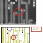
For nearly ten years now, full-chip simulation engines have successfully used process models to perform OPC in production. New full-chip models were regularly introduced as patterning processes evolved to span immersion exposure, bilayer resists, phase shift masking, pixelated illumination… Read More
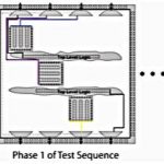
The goal for automatic test pattern generation (ATPG) is to achieve maximum coverage with the fewest test patterns. This conflicts with the goals of managing power because during test, the IC is often operated beyond its normal functional modes to get the highest quality test results. When switching activity exceeds a device’s… Read More
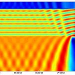
Will Rogers said that an economist’s guess is liable to be as good as anyone’s, but with advanced-node optical lithography, I might have to disagree. Unlike the fickle economy, the distorting effects of the mask and lithographic system are ruled by physics, and so can be modeled.
In this installment, I’ll talk about two critical… Read More
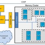
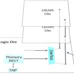
3D ICs complicate silicon testing, but solutions exist now to many of the key challenges. – by Stephen Pateras
The next phase of semiconductor designs will see the adoption of 3D IC packages, vertical stacks of multiple bare die connected directly though the silicon. Through-silicon vias (TSV) result in shorter and thinner… Read More


Oops, we did it again! Memory Companies Investment Strategy