
Extrapolating the trends from last 20 years to the next ten suggests that we will be implementing a trillion transistors or more by 2020. At 20nm, with the chip sizes touching billions of transistors, the age old problem of how to implement a design in the most efficient manner remains unanswered.

Do you do it flat or hierarchical? Are your decisions based on the current tool capabilities or limitations? Is the design being implemented across geographies or locally? Is it a complex SoC or an ASIC? Do you have any 3[SUP]rd[/SUP] party IPs or analog components? Is the market window three months or three years away? In this article we will discuss the requirements of design tools and methodologies to implement such large and complex semiconductors and suggest some approaches to overcome these challenges in an efficient and timely manner.
To illustrate the issue of growing design sizes, take a look at the some of the current big complex chips out there. Graphics processor units (GPU) are some of the biggest designs in production. The latest mobile GPU chips have four to five cores; a new general mobile processor has a total design size near 1 billion transistors[SUP][/SUP]; and another new mobile processor claims to have 4x performance than its previous version and combines a slew of new functionality for the smart phone segment. Not only are these designs extremely large and complex, but they are also developed across teams spread over USA, Europe, India and China, creating another layer of complexity for project management.
Tools and methodologies for the physical implementation of these big designs—from synthesis through place and route, verification, and DFM—have typically taken one of two approaches. The first is a purely flat implementation, the second is a hierarchical implementation. Both the approaches have their own merits and demerits and have worked reasonably well until recently. Moving to 20/14nm, the current tools and methodologies seem to be running out of steam and the design community is looking for a solution that addresses the performance, complexity and time-to-market requirements in addition to handling large amounts of data. A hybrid methodology, a pseudo-flat flow, uses existing tools, technology, and design team infrastructure to enable better results in less time than the traditional flows.
Flat Design Flows
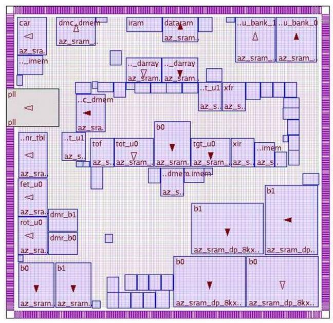
Flat flows have been in vogue since the early days and for good reasons – it is a straightforward flow that provides the best QoR in terms of design utilization and performance. The design is implemented as one entity and typically owned by one engineer. Figure 1 above illustrates a flat design view.
The flat flow starts with pad placement followed by macro placement and fast prototyping. Once the power and ground grid is inserted, the design goes through a couple of iterations of physical synthesis, legalization and then through clock tree synthesis (CTS). Finally the design goes through some further optimization, detail routing, and then final design closure taking into account signal integrity and lithography design variability affects.
This flow works seamlessly as long as the design sizes are reasonably small, less than 4 million gates.. If the design sizes are big (> 5 million gates) the benefits and simplicity of the flat flow are offset by long turn-around-time (TAT) and multiple iterations before design convergence. Yet, there is still a strong push to implement designs whenever possible using this methodology because of the overall silicon efficiency that results from having all the data available so the design tools can make the best tradeoff between design density and performance.
Hierarchical Design Flows
The divide-and-conquer approach of the hierarchical flow is better suited for bigger designs that flat flows cannot handle, or if the design is implemented by different teams in one or more geographies. The goal here is to break down the design into smaller blocks, implement them and then assemble these blocks together at the top level. Figure 2 illustrates a typical hierarchical design view.
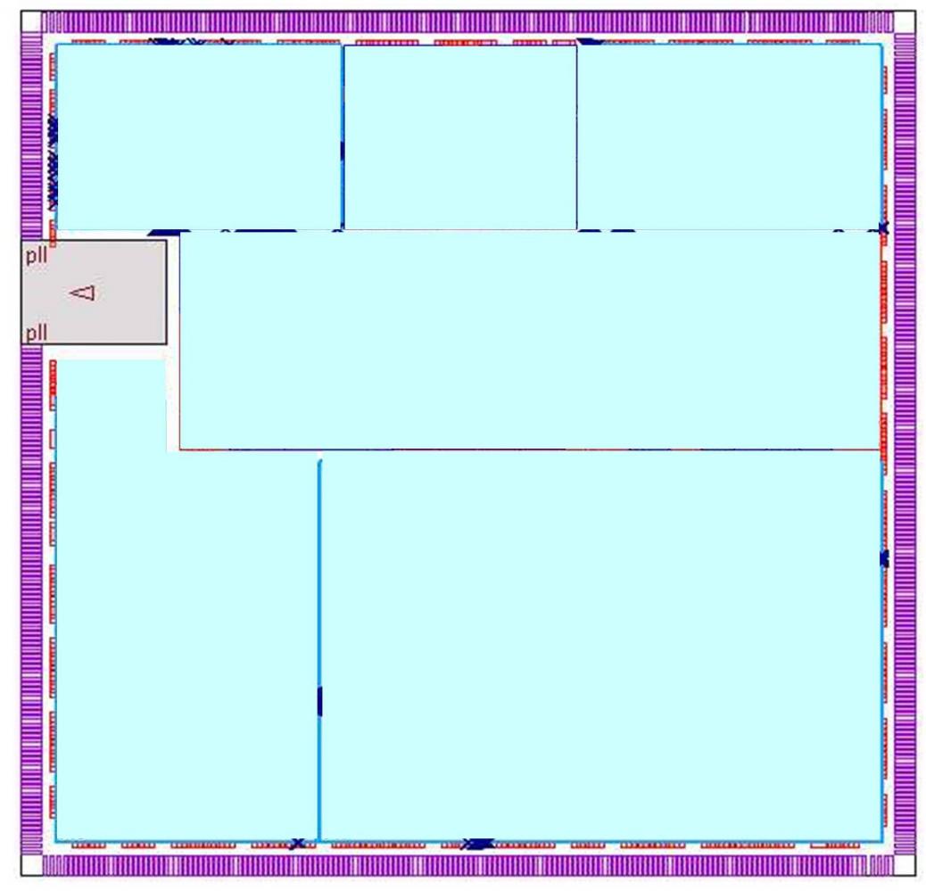
Two general hierarchical approaches are commonly used. The first keeps channels between the different blocks, through which the top-level block interconnects run. But top-level channels and block partitioning result in a loss in area utilization, and an increase in die size to accommodate this top-level routing. Often, the clock speed and skew will not be at par with the flat approach as well. Another challenge with the hierarchical approach is loss in accuracy due to model abstraction that uses models (either ILMs or LIB) of blocks to overcome tool memory limitations. Top-level optimization with these abstracted models leaves performance on the table. Top-level chip assembly poses its own set of problems in terms of timing closure due to poor block-level budget estimates and to the increasing number of mode/corner scenarios. There can also be more CTS insertion delay when the clock trees must go around the different blocks in the top-level channels. This can result in overdesign at the block level, and design teams rarely go back and recover the wasted area and power that was added at the block level to enable top-level timing closure. Estimating clock resources during design planning, optimal pin assignments for each module, generating realistic block-level timing budgets and top-level timing/SI closure are other challenges that need to be considered as part of the hierarchical flow. This again can result in wasted design space if too much area is reserved for this step.
The next style of hierarchical design that has been used is the abutted approach. The advantage of this style is that rather than using channels for top-level routing, the signals are pushed into the blocks themselves. The abutted style offers it’s own challenges in getting these feedthrough signals implemented properly without hurting overall design closure. Plus, it still does not address the issue of overdesign for inter-block timing and power budget closure. It is just attempting to improve the die area problem by reducing channel size. This flow can also pose major challenges for top-level CTS implementation when no top-level channels are present in the design.
Pseudo-Flat Design Flows
Both the hierarchical and flat approaches are at their limits as design sizes grow beyond the 100 million instance mark. In order for the designer to effectively handle these designs without sacrificing performance, power, area, or time-to-results, a hybrid flow, otherwise known as the pseudo-flat approach is becoming essential. The idea here is to break down the design into blocks just as in the hierarchical approach and spawn those blocks off for implementation. Figure 3 shows a pseudo-flat design view.
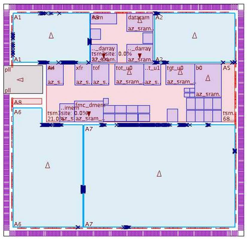
Once the pre-CTS optimization is completed at the block level, the blocks are then merged at the top level and the boundaries removed to optimize the design flat across the entire chip. Selective flattening or preserving blocks based on timing criticality or other IP related issues allows more flexibility to the designer. At this point, the design can proceed through the rest of the flow following the traditional flat design style approach. Most of the heavy lifting in the design flow is during the pre CTS step that was done in a distributed approach. But in order to gain the full benefit of top-level design timing/area/power closure from the flat approach, the design is finalized with a flat design style.
The pseudo-flat flow combines the benefits of the flat and the hierarchical flows, providing good performance and design utilization and fast turnaround times. It also eliminates the inter-block timing modeling inaccuracies associated with the hierarchical flows and results in the most timing- and power-efficient clock trees.
From a design planning perspective, to successfully support the pseudo-flat flow, the physical design tools need to have the capacity to handle top-level optimization of these huge designs and a compact datamodel to minimize the memory footprints discussed earlier, considering clock early during the design planning is critical for fast design convergence, so the tools need to support clock planning as part of the design planning step. Achieving a good macro placement is also critical for extracting the best performance of the design and it should be based on data flow and connectivity analysis.[SUP][ii][/SUP]
It is clear that the design sizes are going to explode as we march down the process nodes, regardless of the end application. For the designers to effectively tackle the design size problem, innovative solutions like pseudo-flat flow will become essential in addition to the current flat and hierarchical approaches.
–Andy Inness
Andy Inness is a place and route specialist at Mentor Graphics, where he applies his 20 years of experience to tool and methodology development for the most advanced designs. Andy received his BSEE from Iowa State University and MSEE from Southern Methodist University. He is based in Austin, TX, but is seen by Mentor customers all over the world.
Estimates vary, ranging from 995 million to 1.16 billion.
[ii] Mentor Graphics whitepaper, “Advanced Floorplanning with Olympus-SoC” describes a mixed-hierarchy, or pseudoflat flow, for floorplanning, macro placement, and pin assignment.
Share this post via:


Comments
0 Replies to “Conquering the Big Data Challenges”
You must register or log in to view/post comments.