You are currently viewing SemiWiki as a guest which gives you limited access to the site. To view blog comments and experience other SemiWiki features you must be a registered member. Registration is fast, simple, and absolutely free so please,
join our community today!
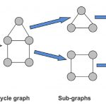
I think by now a lot has been said about the necessity of multi-patterning at advanced technology nodes with extremely low feature size such as 20nm, because lithography using 193nm wavelength of light makes printing and manufacturing of semiconductor design very difficult. The multi-patterning is a novel semiconductor manufacturing… Read More
One of the challenges of physical design of a modern SoC is that of macro placement. Back when a design just had a few macros then the flooplanning could be handled largely manually. But modern SoCs suffer from a number of problems. A new white paper from Mentor covers Olympus-SOCs features to address these issues:
…
Read More
My new iPad lasts about 10 hours on a single charge and the A5X processor is designed with a 45nm process from Samsung. Processor chips for tablets like this use a multi-voltage IC design flow to reduce total power by:… Read More
Conquering the Big Data Challengesby Beth Martin on 04-02-2012 at 4:38 pmCategories: EDA, Siemens EDA
Extrapolating the trends from last 20 years to the next ten suggests that we will be implementing a trillion transistors or more by 2020. At 20nm, with the chip sizes touching billions of transistors, the age old problem of how to implement a design in the most efficient manner remains unanswered. … Read More