While reading an article on DeepChip I found an interesting comment from Rafaela Novais, a Design Support Manager at TowerJazz Semi and decided to interview her to learn more about her experience as an IC designer and EDA tool user.


Q: Where did you get started in IC design?
A: At Motorola I did memory compiler work and got to use a lot of scripting to automate the design and layout tasks. After doing IC design I next moved into the CAD department as an EDA engineer to support other designers.
Q: What came next after Motorola?
A: I moved to San Diego with Zarlink and joined their memory group, where I did some design and verification. In the CAD group we used and supported mixed-signal IC tools.
Q: At TowerJazz what is your role today?
A: My job title is Design Support Manager and I’m the customer liaison in the factory, answering all technical issues from the design customers.
Q: For your customers, what do they receive in a TowerJazz Process Design Kit (PDK)?
A: Our PDK includes symbols and schematics, models (PSP, HICUM, R3, MOS Model 20), info to run Monte-Carlo statistical simulations, Pcells, layout utilities, and a parasitic extraction flow. We show designers how to install, and use the PDK. We also answer process questions, help to add any new devices needed in the PDK, and confirm any bugs.
Q: Which type of PDK does TowerJazz support ?
A: We are supporting both Cadence and iPDK (for Synopsys, Mentor and Tanner tools).
Q: How do TowerJazz customers do their IC designs?
A: Most of our customers are creating AMS designs at the transistor-level, plus we provide digital cell libraries. If they need some design help we have IP development as a design service. They are designing quite a wide range of ICs: ADC, DAC, high voltage, big analog, application-specific, FEM (Front End Module) for wireless and cellular.
Q: In your EDA career why would designers using Data Management (DM) tools?
A: Data Management tools allow a design team to integrate all of the IC design together. With DM tools you can avoid two people modifying the same cell at the same time, and you can lock the cells while working on them. Setting up a new IC design environment we need to have a way to organize our team work areas. It’s essential for modern IC design, we find it pratical and worth the investment, it allows a team to communicate better.
We can recover our place in the IC design process with DM, going back in time if needed.
Redundancy – being able to have the same data available across the whole team, now we can insure that all members have the latest info.
Q: Who on the team would use DM tools?
A: Both schematic design and IC layout would use DM tools. We want to preserve the integrity of the design by using snapshots and tags.
Q: Can you explain more about what a snapshot is?
A: We would save the state of our database before tape-out as a snapshot. We could always go back and make an ECO, or re-use the design, or reference that design in another design.
A snapshot is the state of an IC design database at one point in time, then tagging a design would show all differences made since the last change.
Q: What kind of IC data is controlled by a DM system?
A: Everything: Schematics, layout, test vectors, test benches, RTL files, bug tracking.
Q: When a new designer joined a team, then how would they learn to use DM in the flow?
A: I wrote a how-to guide and would meet with a new engineer to teach them the flow using DM.
Q: When did you start using DM in IC design?
A: I first used a DM at Motorola in 2000, then started using SOS from ClioSoft while at Zarlink (now MicroSemi) in 2002, and it was just starting to get integrated with Cadence Virtuoso. We also used SOS at Luxtera from 2006 to 2011, where they designed silicon photonics in CMOS processes.

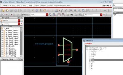
ClioSoft SOS integrated in Cadence Virtuoso
Q: Can a DM help design teams across geographies?
A: Yes, at Zarlink we had multiple locations (San Diego, and Sweden), so we mostly synched the database between locations.
Q: Have you used the Visual Design Diff tool?
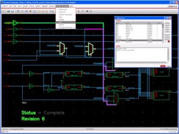
A: Yes, when we need to look at what changed on schematics or IC layouts to quickly find out what changed, and also to verify that what needed to be changed was actually changed.
For schematics we can now see what has changed. If a change is needed for any cell in our library, we now can see the before and after versions to confirm that the ECO was completed.

Schematic Differences

Layout Differences
Q: Who uses VDD?
A: We see the layout designers using it more than the circuit designers. Both groups use VDD to confirm that any change was made.
Summary
Rafaela Novais has an IC design background using many EDA tools and now supports IC design customers at TowerJazz Semi. She has used and supported DM tools like SOS and VDD from ClioSoft.
Also Read
Mixed-Signal Methodology Guide
Book Review: Mixed-Signal Methodology guide
Interview with Brien Anderson, CAD Engineer
Share this post via:


Comments
2 Replies to “EDA User: Rafaela Novais from TowerJazz Semi”
You must register or log in to view/post comments.