
Have you ever heard of a Super Pillar Transistor? It’s one of many emerging 3D transistor types, like Intel’s popular FinFET device.

In the race to continuously improve MOS transistors, these new 3D transistor structures pose challenges to the established IC extraction tool flows.
Foundries have to provide an Effective Profile to EDA companies that describes the shapes used to fabricate any MOS device plus all of the interconnect levels. TCAD tools can be run to simulate what the shapes of an effective profile should be.
How can foundries keep their process proprietary yet provide a geometry for extraction tools to actually use?
Now that’s a constant challenge. I met with Carey Robertson of Mentor Graphics to better understand how the challenges of 3D transistors are being met with the latest generation of IC extraction tools like Calibre xACT 3D.

Q: Intel has an early lead in production-ready 3D FinFETs. When will the Foundries offer FinFETs?
A: The foundries are saying that FinFETS will be used at the 14nm node, however there is much speculation that we could see FinFETS at the 20nm node.
Q: How does a 3D transistor effect the job of IC extraction?
A: The complexity of the effective profile is always increasing, so we have to use more elaborate 3D models that in return require more processing time for detailed extraction used by memory and analog designs.
Q: Will rule-based methods be sufficient in IC extraction?
A: Only for the M1 and higher interconnect layers, for the lower layers near the MOS device you need to really use a field solver to get the accuracy.
Q: How is extraction changing now with 3D?
A: Before we could have a wide distinction between interconnect models and transistor models for parasitics. Now we are using a 3D field solver to extract the R and C values for the MOS source and drain connections.
With 3D devices the MOSFET can even be broken up into multiple fins. We are moving from a table-based and rule-based extraction approach, to explicit calculations. These calculation are just more computational and require longer run times.
Q: What is different about Mentor’s 3D field solver?
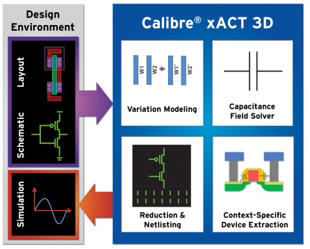
A: Our tool is called xACT 3D and is a field-solver used by designers and is well suited for FinFETS and 3D devices. Caliber xACT 3D has a deterministic field solver (similar to Raphael in the past, although faster), and the output is a SPICE netlist. The extraction input is a GDS II file and foundry decks, so it feels like a standard extraction tool.
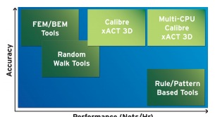
The old Raphael was 1,000x slower than rule-based approaches so is limited to TCAD and small transistor counts.
xACT 3D is maybe 3 to 4x slower than rule-based solvers, however to get results faster you can add more hardware and still stay within 2% of TCAD tool results.
Q: What is the capacity of your 3D field solver?
A: xACT 3D has been run on multi-million transistor memory layouts (see the STARC paper at DAC), flat. It’s not meant for digital sign off. If you want to send the most accurate netlist to SPICE or Fast SPICE for circuit simulation then xACT 3D is the tool for you.
If you want to analyze multi-million digital gates into PrimeTime, then consider a selected net flow.
Q: What is new with xACT 3D this year compared to last year?
A: Well, we have performance improvements (memory up to 4X, analog about 1.5X to 2X), foundry decks at 20nm, more foundry support, plus faster and better viewing of results.
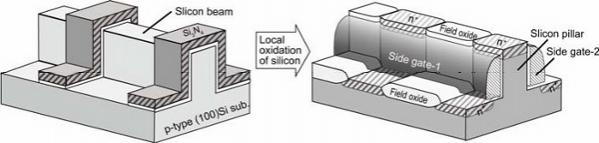
Q: Who would be interested in using a 3D field solver?
A: Memory designers using pillar transistors would need to use a field solver.
Q: Does your field solver work hierarchically?
A: No, it’s not a hierarchical tool although it can read a hierarchical layout and produce a hierarchical netlist.
Q: Will you be presenting at DAC this year?
A: We may be in a panel discussion organized by Ed Sperling, so stay tuned.
Q: What are some other trends happening in IC design today?
A: With Double Pattern Technology (DPT) being used at 20nm it is creating more corners for simulation, so at 28nm we had 5 corners and at 20nm we will have from 11 to 15 corners. More corners means more simulation time.
Q: Who else at Mentor is presenting at DAC this year?
A: Claudia Relyea is presenting with ST in a poster session on 3D extraction.
Karen Chow has a presentation on sensitivity analysis with STARC.
Summary
The DAC conference and trade show is going to be exciting this year as the EDA vendors have adapted their IC design tools to enable design with 3D transistors. Find Mentor Graphics in booth #1530 at DAC.


Comments
One Reply to “3D Transistors and IC Extraction Tools”
You must register or log in to view/post comments.