IC designers have been running analysis tools for power, noise and reliability for many years now, so what is new when you start using FinFET transistors instead of planar transistors? Calvin Chow from ANSYS (Apache Design) presented on this topic earlier in the summer through a 33 minutewebinar that has been archived. There is a brief registration required to view the archived webinar.
Related: FinFET Based Designs Made Easy & Reliable
A quick recap of why FinFET device characteristics at 14nm are better than bulk at 20nm or 28nm include:
- Improved speed
- Reduced power
- Higher device density
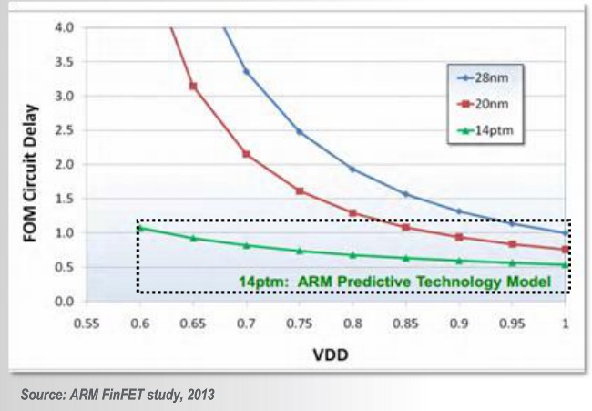
This chart shows performance versus VDD values for three technology nodes: FinFET at 14nm, 20nm planar and 28nm planar:

As the value of VDD lowers, the circuit delay improvement of the FinFET increases versus planar devices. On the downside, FinFET designs add new challenges like:
- Reduced noise margins
- Reduced EM (Electro Migration), ESD (Electro Static Discharge) tolerance
- Increased temperature effects
- Higher device capacity
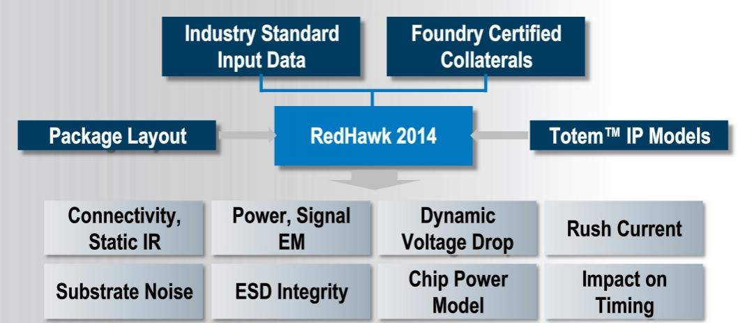
The specific EDA tool that ANSYS offers for power, noise and reliability analysis is called RedHawk 2014 and it addresses each of the new challenges:

Instead of analyzing chip and package separately for IR drop, the recommended approach is a simultaneous analysis using a distributed model of the package instead of a simple, lumped model. Shown below are IR drop analysis results of chip and package, first using a lumped package model which has a 13.8mV drop, next using a distributed package model which shows a more accurate 19.2mV drop value:
Typical runtime to do a package extraction with RedHawk-CPA on a 6 layer package is 10 minutes, while using about 15 GB of RAM. To do the IR drop simulation required just 58 minutes and under 8 GB of RAM.
FinFET Foundries
The FinFET processes at TSMC 16nm v1.0 and the Intel custom foundry at 14nm are certified for use with RedHawk 2014 on the following types of analysis:
- Resistance correlation
- EM rule handling
- IR, Dynamic Voltage Drop extraction and analysis
I would expect support for FinFET processes at Samsung and GLOBALFOUNDRIES in the near future.Related: Intel & ANSYS Enable 14nm Chip Production
Analysis
With higher drive currents, it’s even more important for FinFET designs to have layout checks for connectivity analysis like:
- Missing vias
- Power and ground grid weakness check
- Resistance checks
- Power/Ground balance
- Switch placement
- Pad placement
- IR drop checks
- High power density checks

Reliability analysis includes things like: Electro Migration (EM), thermal and Electro Static Discharge (ESD). Power noise analysis looks for issues of: dynamic voltage drop (DVD) on the power grid, low power compliance with multiple voltage domains, and the impact from power noise on timing. As an example, here’s a plot showing analysis results for timing hotspot and a DVD map, so you can focus first on fixing the IR drop issues in the timing hotspot area:

Summary
The engineers at ANSYS have a long history of building EDA tools for power, noise and reliability analysis. Now they’ve extended that experience into newer IC designs using FinFET technology from foundries like TSMC and Intel using the RedHawk 2014 software release.
Share this post via:


Comments
0 Replies to “FinFET Design for Power, Noise and Reliability”
You must register or log in to view/post comments.