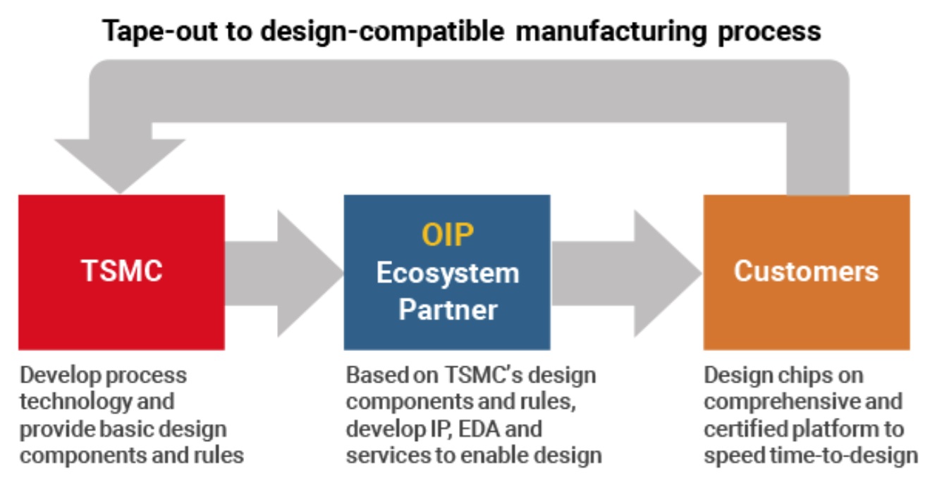
The 2024 live conferences have been well attended thus far and there are many more to come. The next big event in Silicon Valley is the TSMC Global OIP Ecosystem Forum on September 25th at the Santa Clara Convention Center. I expect a big crowd filled with both customers and partners.
This is the 16th year of OIP and it has been an honor to be a part of it. The importance of semiconductor ecosystems is greatly understated as is the importance of the TSMC OIP Ecosystem.
The big change I have seen over the last few years is momentum. The FinFET era has gained an incredible amount of ecosystem strength and the foundation of course is TSMC. When we hit 5nm the tide changed in TSMC’s favor with a huge amount of TSMC N5 EDA, IP, and ASIC services support. In fact, there were a record setting number of tape-outs on this node. This momentum has increased at 3nm with TSMC N3 having the strongest ecosystem support and tape-outs in the history of the fabless ecosystem in my experience.
The momentum is continuing with TSMC N2 which will be the final FinFET node of what has turned out to be an incredible semiconductor era. It is too soon to say what will happen with the angstrom era but my guess is that semiconductor innovation and Moore’s Law will continue in one form or another.
A final thought on the ecosystem, while it appears that IDM foundries have more R&D strength than pure-play foundries I can assure you that is not the case. The TSMC OIP Ecosystem, for example, includes the largest catalog of silicon verified IP in the history of the semiconductor industry. IP companies first develop IP in partnership with TSMC to leverage the massive TSMC customer base. In comparison, the IDM foundries pay millions of dollars to port select IP to each of their processes to encourage customer demand.

Throughout the FinFET era foundries, customers and partners have spent hundreds of billions of R&D dollars in support of the fabless semiconductor ecosystem which will get the semiconductor industry to the one trillion dollar mark by the end of this decade, absolutely.
Here is the event promo:
Get ready for a transformative event that will spark innovations of today and tomorrow’s semiconductor designs at the 2024 TSMC Global Open Innovation Platform (OIP) Ecosystem Forum!
This year’s forum is set to ignite excitement with a focus on how AI is transforming chip design and the latest advances in 3DIC system design. Join industry trailblazers and TSMC’s ecosystem partners for an inside look at the latest innovations and breakthroughs.
Through a series of compelling, multi-track presentations, you’ll witness firsthand how the ecosystem is collaborating to address critical design challenges and leverage AI in chip design processes.
Engage with thought leaders and innovators at this unique event, available both in-person and online across major global locations, including North America, Japan, Taiwan, China, Europe, and Israel.
Don’t miss out on this opportunity to connect with the forefront of semiconductor technology.
Get the latest on:
• Emerging challenges in advanced node design and corresponding design flows and methodologies for N3, N2, and A16 processes..
• The latest updates on TSMC’s 3DFabric chip stacking and advanced packaging technologies including InFO, CoWoS®, and TSMC-SoIC®, 3DFabric Alliance, and 3Dblox standard, along with innovative 3Dblox-based design enablement technologies and solutions, targeting HPC, AI/ML, and mobile applications.
• Comprehensive design solutions for specialty technologies, enabling ultra-low power, ultra-low voltage, analog migration, RF, mmWave, and automotive designs, targeting 5G, automotive, and IoT applications.
• Ecosystem-specific AI-assisted design flow implementations for enhanced productivity and optimization in 2D and 3D IC design.
• Successful, real-life applications of design technologies, IP solutions, and cloud-based designs from TSMC’s Open Innovation Platform® Ecosystem members and TSMC customers to speed up time-to-design and time-to-market.
Also Read:
TSMC’s Business Update and Launch of a New Strategy
TSMC Foundry 2.0 and Intel IDM 2.0
What if China doesn’t want TSMC’s factories but wants to take them out?
Share this post via:


Comments
There are no comments yet.
You must register or log in to view/post comments.