
I’ve used OLED (Organic Light-Emitting Diode) displays for many years in my monitors, laptops, tablets, e-readers and smart phones; and knew that the AMOLED (Active-Matrix OLED) displays used thin-film transistor technology where each pixel can be controlled, but I hadn’t considered the actual design process until Chen Zhao from Empyrean brought up the topic. What follows is part one of a Q&A discussion, where I learned about the design challenges of Flat Panel Design (FPD) and how automation is being applied.
Q: Can you give me a brief history of FPD technology?
After years of persistent efforts, traditional flat panel display (FPD) technology such as liquid crystal display (LCD) has made considerable progress1. Advanced technologies such as organic light-emitting diodes (OLED)2 and flexible panels3 have also make breakthroughs, and the industry share has also greatly increased.
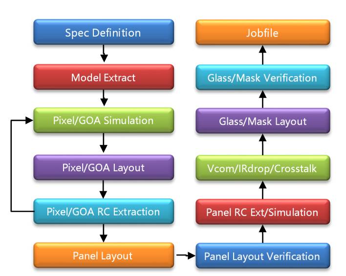
Q: What is the FPD design flow like?
Like integrated circuit design, electronic design automation (EDA) is also the cornerstone of FPD circuit design. The FPD design flow includes panel circuit schematic design, layout design, circuit simulation, circuit layout parasitic parameter extraction, circuit design verification, etc. It is similar to analog integrated circuit design flow, but also has its unique design flow and design methodology.
Q: How was FPD design approached in the early days?
The design flow of early domestic display panels was realized by point tools from multiple EDA tools. Because users need to switch frequently between these manufacturers’ EDA tools, the design flow is cumbersome, data compatibility and confidentiality are not good enough, and problems are not easy to track down. It will cause mutual wrangling, inefficiency, delays in construction, and will deteriorate product quality. In addition, these tools are basically tools from integrated circuit design, and they are obviously lacking in solving the unique professional needs of display panels and customized development.
Q: Instead of using point tools, what is a more efficient and elegant approach?
In order to solve various FPD problems of users, it is urgent to develop an EDA full-flow solution for FPD design. All tools are seamlessly integrated on a unified EDA platform to make the FPD design flow efficient and smooth, ensure design quality, and improve design effectiveness. At the same time, in order to meet the ever-changing design requirements of high-end and new FPD and the customization requirements of domestic customers, it is necessary to continuously develop new functions and new products to improve the leadership of FPD EDA tools.
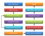
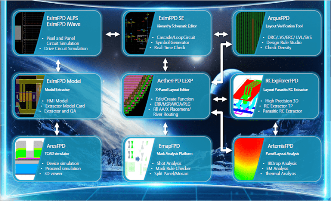
Q: What specific tools has Empyrean put together for the design of FPD?
EMPYREAN has launched the world’s only FPD full-flow design system. Shown below are the main tools of the system, including TCAD, SPICE modeling, circuit schematic design, layout design, circuit simulation, circuit simulation waveform analysis, parasitic RC extraction, layout physics and electrical verification, full design layout analysis, and mask analysis, etc., to achieve full flow coverage, smooth data transfer, and to greatly improve design efficiency.
Q: Does this Empyrean design flow work only for LCD designs?
In addition to achieving the world’s only FPD design full-flow solution, on the basis of meeting LCD conventional design, EMPYREAN keeps up with the forefront of FPD design requirements, especially for the current popular and advanced fields such as curvilinear-shaped design, OLED high-end display, and touch panel4. EMPYREAN has pioneered a series of supporting design technologies, which enable FPD design to a new level and allow display companies to enter the high-end display field.
Q: How are the TFT devices simulated, and what models are being used?
EsimFPD Model is a SPICE model parameter extraction and optimization software specially designed for FPD by EMPYREAN. The traditional thin film transistor (TFT) RPI model has many problems in terms of model accuracy of amorphous silicon (A-Si)5 and low temperature polysilicon (LTPS)6. After years of continuous development and improvement, the R&D team of EMPYREAN has greatly improved the accuracy of the model in terms of temperature effect, sub-threshold area, leakage current and other important device characteristics7.
Taking into account the impact of process fluctuations on device characteristics, we have improved the traditional modeling methodology. Based on a large number of sampled data, we have performed statistical analysis on the device characteristics, and extracted process corner model and statistical model, which will help to reserve the smallest possible reasonable margin for subsequent FPD circuit design, and improve product performance and yield.
Q: What are the challenges of defining an accurate model?
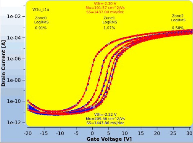
In order to further improve the accuracy of model, based on the geometric dependence of device physics, we considered the geometry dependency of device characteristics with gate length and width of TFT devices, and developed the so-called bin model which can cover big geometry area8.
Our work has been extended to support new devices such as OLED, oxide semiconductor TFT (IGZO)9, and Micro-LED10.
In addition, we support reliability modeling of TFT devices5,6,9, including DC/AC stress model, hysteresis model, and image-sticking model, etc. The device reliability model can be used in circuit simulation tools to analyze the long-term reliability of FPD circuits. The next figure shows the fit of our stress model.
Summary
FPD technology enables many consumer and industrial products that allow us to visualize information every day on our smart phones and monitors, and the design challenges for displays increases with each new product generation. Empyrean has nine tools that work in concert to form a full design flow for FPD products, and in part two I’ll cover topics like:
- Design technology of curvilinear-shaped FPDs
- FPD layout design
- FPD layout verification
- Hierarchical FPD circuit simulation
- RC extraction and analysis
- Thermoelectric analysis
- Mask analysis
- Job file automation
References
- Xiang Feng, Xiao Sun, Qiang Zhang, Dan Wang, “Development Trend of LCD Technology”, Invited Paper, SID Symposium Digest of Technical Papers, 2018
- Ho-Kyoon Chung, Hye-Dong Kim, Boris Kristal, “AMOLED Technology for Mobile Displays”, Invited Paper, SID Symposium Digest of Technical Papers, 2012
- Chang‐Xiang Wu,Yen‐Lin Pan,Hung‐Ming Tsai,“Modeling and Analysis of the Flexible Touch Panel on the Flexible Active-matrix OLED Display”,SID Symposium Digest of Technical Papers, 2014
- Wei-Feng Zhou,Li-Qiang Chen,David Wang,“ New Full Screen Flexible AMOLED Solution with Fingerprint”, Invited Paper, SID Symposium Digest of Technical Papers, 2018
- Ching-Chieh Shih, Yeong-Shyang Lee, Kuo-Lung Fang, Ching-Hung Chen, and Feng-Yuan Gan, “A Current Estimation Method for Bias-Temperature Stress of a-Si TFT Device”, IEEE Trans. Dev. And Mat. Reliability, Vol. 7, No. 2, pp. 347, 2007
- Kim et al, “Investigation of the Instability of Low-Temperature Poly-Silicon Thin Film Transistor under a Negative Bias Temperature Stress”, Electron. Mater. Lett., Vol. 9, 2013
- Lifeng Wu, “An introduction of OLED/TFT device model and FPD design flow”, Invited Paper, MOS-AK Compact Modeling Workshop, Beijing, China, June 2018
- AnThung Cho, Lifeng Wu, Qionghua Mo, James Hsu, Kaijun Liu, Justin, Yunqin Hu, Wade Chen, York Lu, Xiaobin Fan, and Scott Lin, “Corner and Binning Model Simulation of TFT for GOA Driver Circuit in G8.6 Large-size TFT-LCDs”, International Display Workshops, Nagayo, Japan, December 2018
- Ken Hoshino, David Hong, Hai Q. Chiang, and John F. Wager, “Constant-Voltage-Bias Stress Testing of a-IGZO Thin-Film Transistors”, IEEE TRANSACTIONS ON ELECTRON DEVICES, VOL. 56, NO. 7, 1365, JULY 2009
- Brian R.Tull, Nancy Twu, Yu-Jen Hsu, “Micro-LED Micro displays by Integration of III-V LEDs with Silicon Thin Film Transistors”, Invited Paper, SID Symposium Digest of Technical Papers, (246-248), 2017
Also Read
Xilinx Moves from Internal Flow to Commercial Flow for IP Integration


