Moore’s Law has been about device density, specifically transistor density, increasing every certain number of years. Although cost is the most easily grasped advantage, there are two other benefits: higher performance (speed) and reduced power. When these benefits are compromised, they can also pose a scaling limitation. Probably the most well-known scaling limiter for transistors is the short-channel effect (SCE) which has been covered for many years and updated for recent transistor developments like FinFETs. Much less well-known but still very important and persistent is contact resistance, i.e., the electrical resistance of the narrow contact to the much larger transistor. A higher contact resistance is damaging in either of two ways: (1) less current at the same operating voltage, which reduces performance, or (2) higher voltage for the same driving current, which increases power consumption.
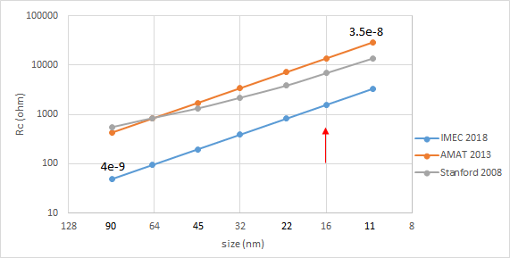
The contact resistance (Rc) is usually characterized by the “contact resistivity” which actually has the units of resistance x area (ohms-cm^2). The actual resistance is computed from contact resistivity by dividing contact resistivity by the contact area. In Figure 1, the trend of contact resistance is plotted from three different references, published over a period of ten years.
Figure 1. Contact resistance trends, from various studies from 2008 to 2018 [1-3].
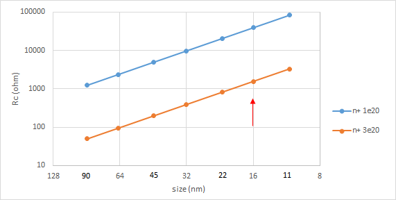
The earliest reference [1] is from 2008, published by Stanford. It was based on projections from the 2005 ITRS roadmap projection at the time. The second reference is from 2013 [2], from an interesting paper discussing the use of an interfacial layer. Half the authors listed were affiliated with Applied Materials, so the data for it on the graph is labeled as “AMAT”. The contact resistivity used here was 3.5e-8 ohm-cm^2. The third, most recent reference is from IMEC[3], which presented an atomistic simulation study. Its values are lower than previous projections. Specific assumptions for this case were: n+ doping of 3e20/cm^3, amorphous titanium silicide interface. The resulting calculated resistivity was 4e-9 ohm-cm^2. A lower doping would raise the resistance significantly (Figure 2). For 1e20/cm^3, with over 2 kOhm resistance, even 65 nm size contacts are a problem for many applications.
Figure 2. The contact resistance can be increased significantly by a reduction of doping (from 3e20/cm^3 to 1e20/cm^3 in this case) [3].
The red arrow in the graph marks where we are today at the bleeding edge. At this point, the contact resistance is already over 1.5 kOhm, and this is about 3 times what it was for the 90 nm node. Contact resistivity needs to get to below 1e-9 ohm-cm^2 to avoid becoming prohibitive at ~10 nm scale. Based on IMEC’s results [3], this may require doping over 1e21/cm^3, which is 2% concentration impact in silicon! It would not be the original pure silicon anymore!
Not surprisingly, the move from planar transistors to FinFETs simultaneously changed the way contacts are landed. They don’t land flat on the silicon surface anymore. Instead the contact lands on and wraps around the angled surfaces of epitaxially grown SiGe, which effectively increases the contact area. In a way, transistor contact scaling in 2D already hit the wall, and we are already operating in 3D.
Notation clarification: The notation “1e20” is the same as 1 x 10^20. Likewise, “3e-8” means 3 x 10^-8.
References
[1] L. Wei, J. Deng, L-W. Chang, K. Kim, C-T. Chuang, H.-S. P. Wong, “Selective Device Structure Scaling and Parasitics Engineering: A Way to Extend the Technology Roadmap,” IEEE Trans. Elec. Dev. 56, 312 (2009).
[2] S. Gupta, P. P. Manik, R. K. Mishra, A. Nainani, M. C. Abraham, S. Lodha, “Contact resistivity reduction through interfacial layer doping in metal-interfacial layer-semiconductor contacts,” J. Appl. Phys. 113, 234505 (2013).
[3] A. Dabral, G. Pourtois, K. Sankaran, W. Magnus, H. Yu, A. de Jamblinne de Meux, A. K. A. Lu, S. Clima, K. Stokbro, M. Schaekers, N. Collaert, N. Horiguchi, M. Houssa, “Study of the Intrinsic Limitations of the Contact Resistance of Metal/Semiconductor Interfaces through Atomistic Simulations,” ECS J. Solid State. Sci. and Tech. 7, N73 (2018).


Siemens U2U 3D IC Design and Verification Panel