Sathyam has over 35 years of experience in company management, R&D management and software development in Electronic Design Automation (EDA) (mostly) and PCB Manufacturing. He has headed companies, global engineering and marketing organizations in Forture-500 and in startups companies to introduce innovative and successful products. He has led startups such as Karthik Electronics, Atrenta and ArchPro Design Automation to successful mergers and acquisitions. His prior management and technical roles were at Avery Design Systems, Atrenta, Synopsys, ArchPro Design Automation BlueSpec, Cadence Design Systems, AT& Bell Labs, Karthik Electronics and Hindustan Teleprinters. Sathyam’s experience in EDA includes SoC Design, Low Power Verification, Electronic System Level Design and Verification, Logic Design Simulation/Formal Verification/Emulation, Fault Simulation and Integrated Circuit Layout Extraction, Design-rule Checking, and Symbolic Layout Compaction. For complete bio of Sathyam please visit his LinkedIn profile.
What brought you to electronics, semiconductors, and EDA?
I was fascinated by electronics in my high school back in the mid-1970s when I built a music stereo system. Later, I got a Bachelors in Electronics at IIT Madras, India and after undergrad did a startup in PCB manufacturing in Chennai, India at the age of 24. Several local magazines in Chennai, India recognized my initiative and wrote articles about me as a promising entrepreneur of the 1982 year. Later, I moved to the US and got a MS in Computer Engineering from Rutgers. I did a design project called “Content Addressable Memory” using UC Berkeley’s Magic Layout tools. It was amazing to see the impact of EDA on helping do designs. That experience jump started my journey with EDA, and after my Masters in Computer Engineering/Computer Science at Rutgers University I joined the famed Electronic Design Automation Department at AT&T Bell Laboratories.
What is Anew Design Automation backstory and when was it launched?
My Co-founder, Dr. Rahul Razdan (Linkedin Profile) when working as the Senior VP of Strategy at Flextronics realized that Long Lifecycle Electronic products faced enormous issues dealing with a semiconductor supply chain dominated by consumer markets. The Long Lifecycle Electronic products covered several market verticals such as aerospace, automobiles, defense, industrial equipment, medical, power and energy, IoT, and telecom. Specific issues included reliability, semiconductor obsolescence, and evolving maintenance functionality.
More recently, Rahul was awarded the Hall of Fame Honors by the ACM for his Ph. D work at Harvard University on reconfigurable computing. He realized that AI/ML and reconfigurable computing techniques could be used to solve the issues of reliability, supply-chain obsolescence, and functionality obsolescence.
Rahul and I had worked together at Cadence Design Systems where we had successfully delivered flagship products such as Incisive and AMS platforms to the marketplace. In July of 2020, we founded Anew Design Automation with me as President and CEO and with Rahul as the Chairman and Chief Technical Advisor. Interestingly, we have discovered that along the way, system board design also needed to be upgraded, and our critical IP could accelerate this task as well.
As CEO, I brought on board another EDA veteran, Faiq Fazal (Linkedin Profile) as VP Engineering in October 2020 to lead the engineering efforts, and we have built a strong team of ten engineers with expertise in design, AI/ML, Database, GUI, and of course EDA. Interestingly, the original NC-Verilog engineering team which I managed at Cadence Design Systems was about the same size, and that platform has delivered over $1Billion in revenue and counting.
What customer challenges are you addressing?
LLC (Long Lifecycle) customers face a design environment which has not changed very much over several decades, yet the design challenges have accelerated. Today, the role of programmable devices such as FPGAs, programmable processor cores, programmable analog cores, microprocessors has significantly increased. Also, in most embedded design, the dominant design element is the software stack and associated ecosystem for their vertical market. For designers, they face a sea of information spread across websites, EDA databases, reference designs, and application notes. Amazingly, the central repository of information is still the datasheet, and PDF search is the EDA tool of choice. Our previous articles on Semiwiki describe this situation in detail. Anew will be addressing this problem with advanced semiconductor component selection through design intent, design abstraction, and design related linting.
After the initial design, LLC customers face a couple of specific pain points:
- Say the product has been launched to market. Significant resources have been spent on qualification, certification, system validation and the product is being actively used by customers. There are active maintenance contracts and warranties connected to the system design. Five years later, there is a semiconductor obsolescence or reliability problem. The design team is long gone, and the leadership is left with difficult and expensive choices.
- When the product is embedded into infrastructure or distributed out in the field. The cost of updating the hardware is expensive or even impossible (think satellites).
Anew addresses these issues through a Design for LLC flow. Details of the approach can be found on EPSNews Articles and details of the company can be found at www.anew-da.ai. The leadership team consists of EDA (Cadence, Synopsys) veterans who have built highly differentiated solutions which were not available in the marketplace. In summary, Anew solves the pain points for electronics design engineering and component management functions for Long Lifecycle Electronic products companies in vertical markets such as aerospace, automobiles, defense, industrial equipment, IoT, medical, power and energy and telecom.
What is your competitive positioning?
Interestingly, Anew seems to be in a gap of functionality between the major parts of the electronics ecosystem. The key players include:
- PLM Companies: PLM (Product Level Management) is very important to LLC customers and the conventional PLM solutions are well integrated. However, PLM capability does not address the specific electronic design challenges described above.
- EDA Companies: EDA has an intense focus on semiconductor design. Even today, PCB design tools are still operating in a component structure model with little regard for the current issues of system board designers.
- Distributors: Distributors such as Digi-Key and Mouser serve as smart searchers for components, but of course this does not address the core design issues around soft IP, programmable hardware or software.
Anew sits in the large and growing gap between these pillars of conventional functionality with a solution leveraging critical AI/ML and reconfigurable computing technology.
What is the funding situation for Anew?
The company has raised a seed round of around $100K sufficient to do develop the product ideas, functional specifications and a prototype. Currently, we are working on raising $1M+ through institutional investors, angel investors, and US government grants to productize the first product, System Level Design (SLD) Explorer Smart Searcher.
What does the coming months/years have in store for Anew?
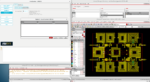
We have conceptualized a powerful EDA platform in which we plan on releasing a series of product releases towards a solution which can solve these deep Long Life Cycle Product issues. As you might imagine, in the coming months, we are hyper focused on building the first product: SLD Explorer Smart Searcher. The figure below should give you a sense of the product architecture and process flow for this product. We have walked senior designers in the defense, medical, and energy markets through this product, and gotten very positive feedback. We expect to release this product to the marketplace in Q221.
Finally, in terms of a call-to-action. We are very interested in engaging with potential partners such as distributor, semiconductor, EMS, or EDA companies who find our value statement of interest. Also, we would love to engage with design teams who want to work with an innovative company to accelerate their productivity.
Also Read:
CEO Interview: Pim Tuyls of Intrinsic ID