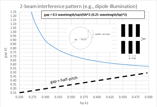
Pretty much all the semiconductor nodes in the last two decades have had at least one layer where the minimum pitch pushes the limitation of the state-of-the-art lithography tool, with a k1 factor < 0.5, i.e., the half-pitch is less than 0.5*wavelength/numerical aperture. A number of published reports [1-4] have touched upon the fact that for such tight pitches, the line end gaps tend to widen. The proof outlined briefly here with reference to the figure below is actually an alternative formulation to the one given in the appendix of [1].
The pitch is defined by illumination distributed about the ideal angle, with a sine of 0.5*wavelength/pitch. The numerical aperture naturally limits the sine in the perpendicular direction to sqrt(NA^2 – (0.5 wavelength/pitch)^2) or sqrt(NA^2 – (0.25 wavelength/half-pitch)^2). From the Fourier diffraction theory, related to the well-known single-slit aperture diffraction problem [5], the minimum width of the gap, correlating to this maximum perpendicular sine is 0.5*wavelength/sqrt(NA^2 – (0.25 wavelength/half-pitch)^2). This is plotted as the blue curve in the figure. k1 is defined as the size divided by wavelength/numerical aperture.
From the graph, it is noted that the gap will always exceed the half-pitch (indicated by the black dotted line in the figure), when the half-pitch is less than 0.5 wavelength/numerical aperture. Moreover, the smaller the half-pitch, the larger the minimum gap. This brings up some basic issues. First, the device density cannot improve much, as the widening gap offsets the shrinking line pitch. Additionally, for the metal interconnections, the next layer with the same line pitch cannot make the connections, as the required gap is too wide. Consequently, there is a need to use separate exposures to cut the line [1] or even stitch the perpendicular features at the same target pitch [2]. The latter has been promoted for bidirectional layouts by ASML as double dipole exposure lithography [2,6]. On the other hand, for unidirectional layouts, separate line cuts have become the norm, due to less stringent overlay requirements.
References
[1] https://semiwiki.com/lithography/285085-lithography-resolution-limits-line-end-gaps/
[2] M. Eurlings et al., Proc. SPIE 4404, 266 (2001).
[3] M. Burkhardt et al., Proc. SPIE 7274, 727404 (2009).
[4] E. van Setten et al., Proc. SPIE 9661, 96610G (2015).
[5] B. E. A. Saleh and M. C. Teich, Fundamentals of Photonics, John Wiley & Sons, 1991, pp.128-129.
[6] S. Hsu et al., Proc. SPIE 4691, 476 (2002).
Share this post via:


Is Intel About to Take Flight?