You are currently viewing SemiWiki as a guest which gives you limited access to the site. To view blog comments and experience other SemiWiki features you must be a registered member. Registration is fast, simple, and absolutely free so please,
join our community today!
The Siemens Calibre group was very busy last week at SPIE. Calling Calibre industry leading really is an understatement. Calibre is one of the reasons Moore’s Law has continued to this day. This tool is legendary. You can get more information on the Calibre landing page including product information, resource guide, blogs
…
Read More
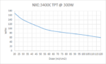
Recently, a patent application from TSMC [1] revealed target EUV doses used in the range of 30-45 mJ/cm2. However, it was also acknowledged in the same application that such doses were too low to prevent defects and roughness. Recent studies [2,3] have shown that by considering photon density along with blur, the associated shot… Read More
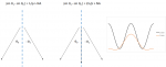
Recent advances in EUV lithography have largely focused on “low-k1” imaging, i.e., features with pitches less than the wavelength divided by the numerical aperture (k1<0.5). With a nominal wavelength of 13.5 nm and a numerical aperture of 0.33, this means sub-40 nm pitches. It is naturally expected that larger… Read More
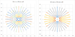
Due to the higher energy of EUV (13.3-13.7 nm wavelength) compared to ArF (193 nm wavelength) light, images produced by EUV are more susceptible to photon shot noise.
Figure 1. (Left) 40 nm dense (half-pitch) line image projected onto wafer at 35 mJ/cm2; (Right) 20 nm dense (half-pitch) line image projected onto wafer at 70 mJ/cm2.… Read More
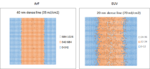
At the SPIE Advanced Lithography Conference held in February, ASML presented the latest information on their Deep Ultraviolet (DUV) and Extreme Ultraviolet (EUV) exposure systems. I recently got to interview Mike Lercel of ASML to discuss the presentations.
DUV
Despite all the attention EUV is getting, most layers are still… Read More
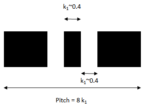
Pretty much all the semiconductor nodes in the last two decades have had at least one layer where the minimum pitch pushes the limitation of the state-of-the-art lithography tool, with a k1 factor < 0.5, i.e., the half-pitch is less than 0.5*wavelength/numerical aperture. A number of published reports [1-4] have touched upon… Read More
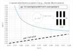
In an earlier article [1], the resolution limit for the space between paired features was described by the Rayleigh criterion of ~0.6 wavelength/numerical aperture, where the numerical aperture (NA) represented the sine of the largest angle for a ray focused from the lens to a point. It is also given by the radius of the lens divided… Read More
State-of-the-art chips will always include some portions which are memory arrays, which also happen to be the densest portions of the chip. Arrayed features are the main targets for lithography evaluation, as the feature pitch is well-defined, and is directly linked to the cost scaling (more features per wafer) from generation… Read More
The current leading edge of advanced lithography nodes (e.g., “7nm” or “1Z nm”) features pitches (center-center distances between lines) in the range of 30-40 nm. Whether EUV (13.5 nm wavelength) or ArF (193 nm wavelength) lithography is used, one thing for certain is that the minimum imaged pitch … Read More
The annual SPIE Advanced Lithography Conference kicked off last night with vendor sponsored networking events and such. SPIE is the international society for optics and photonics but this year SPIE Advanced Lithography is all about the highly anticipated EUV technology. Scotten Jones and I are at SPIE so expect more detailed… Read More