We have seen that the interface IP category is seeing incredibly high growth rate over the last two decades and we expect this category to generate an ongoing high source of IP revenues for at least another decade. But if we dig into the various successful protocols like PCI Express, Ethernet or USB, we can detect a common function in the Physical (PHY) part, the Serializer/Deserializer (SerDes) function.
In 1998, advanced interconnects used in telecom application were based on 622 MHz LVDS I/O. Telecom chip makers were building huge chips integrating 256 LVDS I/O running at 622 MHz to support Networking fabric. Today, advanced PAM4 SerDes run at 112 Gbps; over a single connection to support 100G Ethernet. In twenty years, SerDes technology efficiency jumped by a factor of 180-times! If we make a quick comparison with CPU technologies. In 1998 Intel released the Pentium II Dixon processor, whose frequency was 300 MHz. In 2018, an Intel Core i3 run at 4 GHz. CPU frequencies have grown by a factor of 15 times over a span of twenty years while SerDes speeds have exploded by by a factor of 180-times.
SerDes are now used in many more application than just telecom, to interface chips and systems. At the end of the 2000’s, smartphones integrated USB3, SATA and HDMI interfaces, while Telecom and PC/server integrated both PCIe and Ethernet. These trends resulted in the interface IP market to become a sizeable IP category growing above $200 million at that time. It was small compared to the CPU category, which was four or five times larger. But, since 2010, the interface category has seen at least 15%, year over year. It was the fastest growing category compared with all other semiconductor IP categories, such as CPU, GPU, DSP, Library, etc. The reason is directly linked with the number of connected devices growing every year, each exchanging more data (more movie, pictures, etc.). Connectivity is the beginning of the chain of communication, to the internet modem or base station, Ethernet switch and the datacenter network.
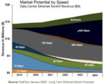
Figure 1: Long Term Ethernet Switch Forecast (source: Dell’Oro)
During the 2010 decade the worldwide community became almost completely connected. Ethernet became the backbone of this connectivity as both the connectivity rates and the number of datacenter quickly increased over the decade. If we use SerDes rates as an indicator, it was 10 Gbps in 2010, 28 Gbps in 2013 and 56 Gbps in 2016 (allowing to support 10G, 25G and 50G Ethernet resp.) and 112 Gbps in 2019.
Then, in 2017, the exploding high-speed connectivity needs for emerging data-intensive compute applications such as machine learning and neural networks started to appear, adding to the growing need of high bandwidth connectivity. At the same time, analog mixed-signal architectures, which were the norm for SerDes design since the inception, became extremely difficult to manage and much more sensitive to process, voltage, and temperature variations, due to the evolution of CMOS technology toward advanced FinFET. In modern nanometer FinFET technologies, building transistors involves stacking individual electrons, given the tiny dimensions of the transistors. Thus, the construction of precise, analog circuits that can sustain stressful environmental variations is extremely difficult.
But the positive point with advanced technology like 7nm is that you can integrate an incredible number of transistors by sq. mm (density of 100 million Transistor per sq. mm), so it’s now possible to develop new digital-based architecture leveraging Digital Signal Processing (DSP) to do the vast majority of the Physical Layer work. DSP-based architecture enables the use of higher order Pulse Amplitude Modulation (PAM) modulation scheme compared to Non-Return to Zero (NRZ or PAM2) used by historical previous analog mixed-signal approaches. PAM 4 enabled doubling data throughput of channels without having to increase the bandwidth of channels themselves. As an example, a channel with 28 GHz of bandwidth can support a maximum data throughput of 56 Gbps using NRZ signaling. With the use of PAM-4 DSP technique this same 28 GHz bandwidth channel can now support a data rate of 112 Gbps! When you consider that analog SerDes architectures are limited to a maximum of 56 Gbps rates for physical reasons (and maybe less…), DSP SerDes are the approach to scale rates to 200 Gbps and beyond, with the use of more sophisticated modulation schemes (eg. PAM-6 or PAM-8).
Using DSP based SerDes is not only required for building robust interfaces in FinFET technologies, but it is also the only way to double data rates for above 56 Gbps, eg. 112 Gbps with PAM-4, 200 Gbps with PAM-8. And this need for more bandwidth is the requirement linked with emerging data-intensive applications like AI (to interconnect CPU and accelerator), ADAS, and to follow the data-centric trend of the connected human community, expected to grow steadily over the next decade.
Figure 2: Top 5 Interface IP Forecast & CAGR (source: IPnest 2020)
In the “Interface IP Survey” IPnest rank the market share of IP vendor revenues by protocol since 2009. In the 2020 version of the report, we have shown that the Interface IP category will have 15% CAGR from 2020-2024 to reach $1.57 billion, as listed in Figure 2. This is a wide IP market including PCIe, Ethernet and SerDes as well as USB, MIPI, HDMI, SATA and memory controller IP. In 2019, Synopsys is a strong leader with 53% market share of the estimated $870 million IP market, followed by Cadence with 12%. Both EDA companies have defined a one-stop-shop business model, addressing the mainstream market. This strategy is successful for these large companies as it targets a wide part of various segments (smartphone, consumer, automotive or datacenter), but not the most demanding high-end portion of these segments.
Nevertheless, another strategy can be successful for the IP market, which is to strongly focus on one segment (eg. High-end) of the market and provide the best experience to very demanding hyperscalar customers. If you can build an excellent engineering team able to develop top quality products on the most advanced technologies, focusing on the high end of the market, the resulting business model can be rewarding.
We have seen that SerDes IP is the key to the interface IP market. Furthermore if we concentrate on PCIe and Ethernet protocols, Figure 3 illustrates the IP revenues forecast 2020-2025, limited to high-end PCIe (Gen 5 and Gen 6) and high-end Ethernet (PHY based on 56G, 112G and 224G SerDes), including D2D protocol for a reason that will be describes shortly.
Figure 3: High-End Interface IP Forecast & CAGR (source: IPnest 2021)
This high-end interface IP forecast show 28% CAGR from 2020-2025 (to be compared with 15% for the total interface IP market), and a TAM of $806 million in 2025. One young company has demonstrated strong leadership on this High-End interface IP segment, thanks to their focus on high-end SerDes (112G since 2017 and soon 200G) targeting the most advanced technology nodes (7nm in 2017, then 5nm in 2019) offered by the two leading foundries, TSMC and Samsung. Alphawave, was founded in 2017 has are rumored to have $75 million in orders in 2020, thanks to their positioning targeting the most advanced rates and application of the high-end segment of PCIe and Ethernet. In this portion of the market, they enjoyed 28% market share in 2019 and 36% in 2020. If Alphawave can keep their advance on the high-end SerDes market, it’s not unrealistic to foresee $300-400 million in IP revenues… by 2024-2025!
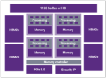
Since 2019, a new sub-segment, D2D interface, has emerged and is expected to grow with 46% CAGR from 2020-2024. By definition, D2D protocol are used between two chips or die, within a common silicon package. Briefly, we consider two cases for D2D: i) dis-integration of the master SoC to avoid SoC area to badly impact yield or become larger that the maximum reticle size, or ii) SoC interconnect with “service” chiplet (can be I/O chip, FPGA, accelerator…).
At this point (February 2021), there are several protocols being used, with the industry trying to build formalized standards for many of them. Current leading D2D standards includes i) Advanced Interface Bus (AIB, AIB2) initially defined by Intel who has offered royalty free usage, ii) High Bandwidth Memory (HBM) where DRAM dies are stacked on each other on top of a silicon interposer and are connected using TSVs, iii) Domain-Specific Architecture (ODSA) subgroup, an industry group, has defined two other interfaces, Bunch of Wires (BoW) and OpenHBI. All of these D2D standards are based on DDR-like protocol, a parallel group of single-ended data wires being accompanied with a forwarded clock currently operating in the the 2GHz to 4 GHz range. By using literally hundred of parallel wires over very short distances, these interfaces compete with VHS SerDes NRZ, usually defined around 40 Gbps, and offering a strong advantage to enable a much lower latency and lower power consumption, compared to SerDes.
There is now consensus in the industry that a maniacal focus on achieving Moore’s law is becoming not valid anymore for advanced technology node, eg. 7nm and below. Chip integration is still happening, with more transistor being added per sq. mm at every new technology node. However, the cost per transistor is growing higher every new node. Chiplet technology is a key initiative to drive increased integration for the main SoC while using older mainstream nodes for service chiplet. This hybrid strategy decreases both the cost and the design risk associated with integration of the service IP directly into the main SoC. IPnest believes this trend will have two main effect in the interface IP business, one will be the strong growth of D2D IP revenues soon (2021-2025), and the other is the creation of the heterogenous chiplet market to augment the high end SerDes IP market.
We have forecasted the growth of the D2D Interface IP category for 2020-2025, passing from less than $10 million in 2020 to $171 million in 2025 (87% CAGR). This forecast is based on the assumption that the service chiplet market should explode in 2023, when most of advanced SoC will be designed in 3nm. This will make integration of high-end IP like SerDes far too risky, leading to externalizing this functionality into a chiplet designed in more mature node like 7 or 5nm. If Interface IP vendors will be major actors in this revolution, the Silicon foundries addressing the most advanced nodes like TSMC and Samsung and manufacturing the main SoC will have key role. We don’t think they will design chiplet, but they could make the decision to support IP vendors and push them to design chiplet to be used with SoC in 3nm, like they do today when supporting advanced IP vendors to market their high-end SerDes as hard IP in 7nm and 5nm. Intel’s recent transition to 3rd party foundries is expected to also leverage third party IPs, as well as heterogenous chiplet adoption by the semiconductor heavyweight. In this case, no doubt that Hyperscalars like Microsoft, Amazon and Google will also adopt chiplet architecture… if they don’t even precede Intel in chiplet adoption.
By Eric Esteve (PhD.) Analyst, Owner IPnest
Also Read:
Interface IP Category to Overtake CPU IP by 2025?
Design IP Revenue Grew 5.2% in 2019, Good News in Declining Semi Market
#56thDAC SerDes, Analog and RISC-V sessions