The vast majority of the attention given to the introduction of each new advanced process node focuses on lithographic updates. The common metrics quoted are the transistors per mm**2 or the (high-density) SRAM bit cell area. Alternatively, detailed decomposition analysis may be applied using transmission electron microscopy (TEM) on a lamella sample, to measure fin pitch, gate pitch, and (first-level) metal pitch.
With the recent transition of the critical dimension layers from 193i to extreme ultraviolet (EUV) exposure, the focus on litho is understandable. Yet, process development and qualification encompasses many more facets of materials engineering to achieve robust manufacturability, so that the full complement of product goals can be achieved. Specifically, process development engineers are faced with increasingly stringent reliability targets, while concurrently achieving performance and power dissipation improvements.
At the recent IEDM conference, TSMC gave a technical presentation highlighting the development focus that enabled the N5 process node to achieve (risk production) qualification. This article summarizes the highlights of that presentation. [1]
An earlier SemiWiki article introduced the litho and power/performance features of N5. [2] One of the significant materials differences in N5 is the introduction of a “high mobility” device channel, or HMC. As described in [2], the improved carrier mobility in N5 is achieved by the introduction of additional strain on the device channel region. (Although TSMC did not provide technical details, the pFET hole mobility is also likely improved by the introduction of a moderate percentage of Germanium into the Silicon channel region, or Si(1-x)Ge(x).)
Additionally, the optimized N5 process node incorporates an optimized high-K metal-gate (HKMG) dielectric stack between gate and channel, resulting in a stronger electric field.
A very significant facet of this “bandgap engineering” for carrier mobility and the gate oxide stack materials selection is to ensure that reliability targets are satisfied. Several of the N5 reliability qualification results are illustrated below.
TSMC highlighted the following reliability measures from the N5 qualification test vehicle:
- bias temperature stability (BTI)
- both NBTI for pFETs and PBTI for nFETs, manifesting in a performance degradation over time from a device Vt shift (positive absolute value) due to trapped oxide charge
- also may result in a degradation of VDDmin for SRAM operation
- hot carrier injection (HCI)
- an asymmetric injection of charge into the gate oxide near the drain end of the device (operating in saturation), resulting in degraded carrier mobility
- time-dependent gate oxide dielectric breakdown (TDDB)
Note that the N5 node is targeted to satisfy both high-performance and mobile (low-power) product requirements. As a result, both performance degradation and maintaining an aggressive SRAM VDDmin are important long-term reliability criteria.
TDDB
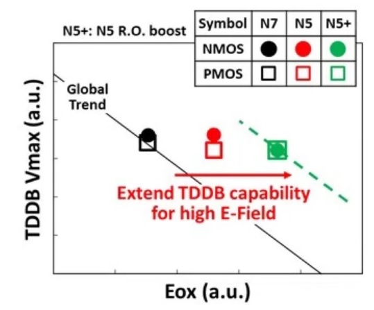
The figure above illustrates that the TDDB lifetime is maintained relative to node N7, even with the increased gate electric field.
Self-heating
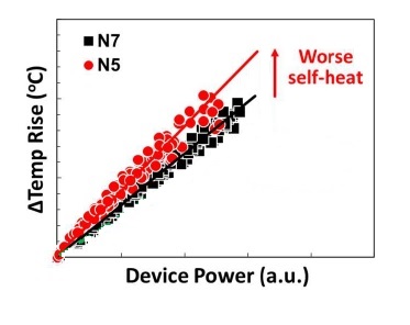
The introduction of FinFET device geometries substantially altered the thermal resistance paths from the channel power dissipation to the ambient. New “self-heating” analysis flows were employed to more accurately calculate local junction temperatures, often displayed as a “heat map”. As might be expected with the aggressive dimensional scaling from N7 to N5, the self-heat temperature rise is greater in N5, as illustrated below.
Designers of HPC products need to collaborate with both their EDA partners for die thermal analysis tools and their product engineering team for accurate (on-die and system) thermal resistance modeling. For the on-die model, both active and inactive structures strongly influence the thermal dispersion.
HCI
Hot carrier injection performance degradation for N7 and N5 are shown below, for nFETs and pFETs.
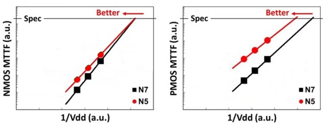
Note that HCI is strongly temperature-dependent, necessitating accurate self-heat analysis.
BTI
The pMOS NBTI reliability analysis results are illustrated below, with the related ring oscillator performance impact.
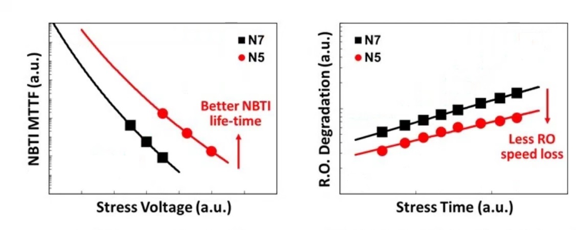
In both cases, reliability analysis demonstrates improved BTI characteristics of N5 relative to N7.
SRAM VDDmin
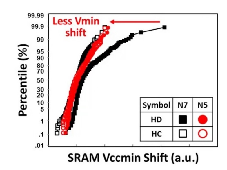
The SRAM minimum operating voltage (VDDmin) is a key parameter for low-power designs, especially with the increasing demand for local memory storage. Two factors that contribute to the minimum SRAM operating voltage (with sufficient read and write margins) are:
- the BTI device shift, as shown above
- the statistical process variation in the device Vt, as shown below (normalized to Vt_mean in N7 and N5)
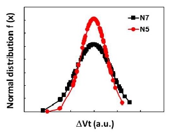
Based on these two individual results, the SRAM reliability data after HTOL stress shows improved VDDmin impact for N5 versus N7.
Interconnect
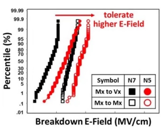
TSMC also briefly described the N5 process engineering emphasis on (Mx, low-level metal) interconnect reliability optimization. With an improved damascene trench liner and a “Cu reflow” step, the scaling of the Mx pitch – by ~30% in N5 using EUV – did not adversely impact electromigration fails, nor line-to-line dielectric breakdown. The figure below illustrates the line-to-line (and via) cumulative breakdown reliability fail data for N5 compared to N7 – N5 tolerates the higher electric field with the scaled Mx pitch.
Summary
The majority of the coverage associated with the introduction of TSMC’s N5 process node related to the broad adoption of EUV lithography to replace multipatterning for the most critical layers, enabling aggressive area scaling. Yet, process engineers must also optimize materials selection and many individual fabrication steps, to achieve reliability targets. TSMC recently presented how these reliability measures for N5 are superior to prior nodes.
-chipguy
References
[1] Liu, J.C., et al, “A Reliability Enhanced 5nm CMOS Technology Featuring 5th Generation FinFET with Fully-Developed EUV and High Mobility Channel for Mobile SoC and High Performance Computing Application”, IEDM 2020.
Share this post via:


Comments
One Reply to “Advanced Process Development is Much More than just Litho”
You must register or log in to view/post comments.