You are currently viewing SemiWiki as a guest which gives you limited access to the site. To view blog comments and experience other SemiWiki features you must be a registered member. Registration is fast, simple, and absolutely free so please,
join our community today!
As industries become more reliant on advanced technologies, the importance of ensuring the reliability and longevity of critical systems grows. Failures in components, whether in autonomous vehicles, high performance computing (HPC), healthcare devices, or industrial automation, can have far-reaching consequences.… Read More
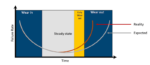
Semiconductor chips are all tested prior to shipment in order to weed out early failures, however there are some more subtle reliability effects that only appear in the longer term, like clock aging. There’s even a classic chart that shows the “bathtub curve” of failure rates over time:
If reality and expectations… Read More
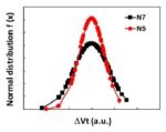
We all know that designers work hard to reach design closure on SOC designs. However, what gets less attention from consumers is the effort that goes into ensuring that these chips will be fully operational and meeting timing specs over their projected lifetime. Of course, this is less important for chips used in devices with projected… Read More
The vast majority of the attention given to the introduction of each new advanced process node focuses on lithographic updates. The common metrics quoted are the transistors per mm**2 or the (high-density) SRAM bit cell area. Alternatively, detailed decomposition analysis may be applied using transmission electron microscopy… Read More
It might seem I am straying from my normal beat in talking about implementation; after all, I normally write on systems, applications and front-end design. But while I’m not an expert in implementation, I was curious to understand how the trending applications of today (automotive, AI, 5G, IoT, etc.) create new demands on implementation,… Read More
At Intel back in the late 1970’s we wanted to know what process corner each DRAM chip and wafer was trending at so we included a handful of test transistors in the scribe lines between the active die. Having test transistors meant that we could do a quick electrical test at wafer probe time to measure the P and N channel transistor… Read More
In a former life I was the GM of a business where we built specialized structures used for semiconductor process bring-up, characterization and monitoring. These monitoring structures were placed in wafer scribe-lines and were used to monitor key parameters during wafer processing. The structures provided feedback to automated… Read More
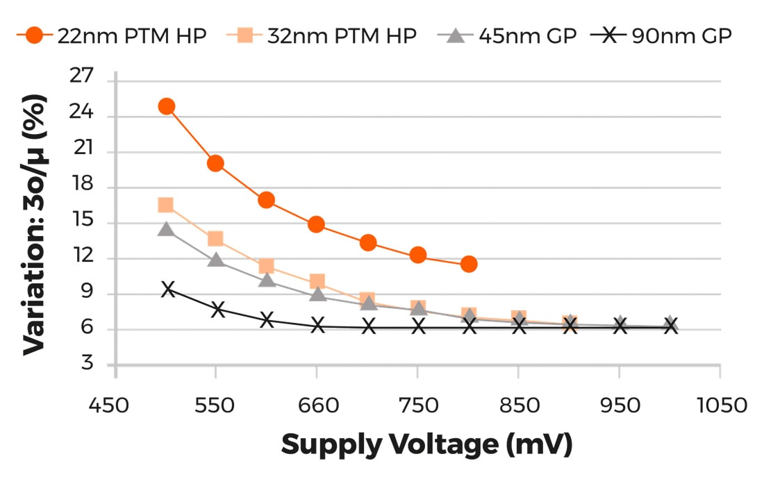
Technology trends make the concerns with electronic noise a primary constraint that impacts many mainstream products, driving the need for “Design-for-Noise” practices. That is, scaling, and the associated reduction in the device operating voltage and current, in effect magnifies the relative importance of non-scalable… Read More
At the recent TSMC OIP symposium, a collaborative presentation by Synopsys and Xilinx highlighted the importance of incorporating the local FinFET device self-heating temperature increase on the acceleration of device reliability mechanisms.… Read More