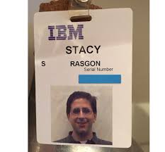
Bloomberg did an interview with my favorite semiconductor analyst Stacy Rasgon on “How the Number One U.S. Semiconductor Company Stumbled” that I found interesting. Coupled with the Q&A Bob Swan did at the Credit Suisse Annual Technology Conference I thought it would be good content for a viral blog.

Stacy Rasgon is an interesting guy and a lot like me when it comes to offering blunt questions, observations, and opinions that sometimes throw people off. As a result, Stacy is not always the first to ask questions during investor calls and sometimes he is not called on at all which is the case for the most recent Intel Call.
Stacy is the Managing Director and Senior Analyst, US Semiconductors, for AB Bernstein here in California. Interestingly, Stacy has a PhD in Chemical Engineering from MIT, not the usual degree for a sell side analyst. Why semiconductors? Stacy did a co-op at IBM TJ Watson Research Center during his post graduate studies and that hooked him.

I thought it was funny back when Brian Krzanich (BK) was CEO of Intel. BK has a Bachelor’s Degree in Chemistry from San Jose State University and he was answering questions by an analyst with a PhD from MIT. The current Intel CEO Bob Swan is a career CFO with an MBA so maybe that explains the communication issues.
In the Bloomberg interview the focus was on the delays in the Intel processes starting with 14nm, 10nm, and now 7nm. Unfortunately they missed the point. In the history of the semiconductor industry leading edge processes were more like wine where in the words of the great Orson Wells “We will sell no wine before its time”. Guided by Moore’s Law, Intel successfully drove down the bumpy process road until FinFETs came along.
The first FinFET Process was Intel 22nm which was the best kept secret in semiconductor history. We don’t know if it was early or late since it was not discussed before it arrived. 14nm followed which was late due to defect density/yield problems. We talked about that on SemiWiki quite and I had a bit of a squabble with BK at a developer conference. I knew 14nm was not yielding and he said it was only to retract that comment at the next investor call. Intel 10nm is probably the most tardy process in the history of Intel and now 7nm is in question as well.
The foundries historically have been 1-2 nodes behind Intel so they got a relative pass on being late with new processes up until 10nm when TSMC technically caught Intel 14nm.
Bottom line: Leading edge processes use new technology and materials which challenges yield from many different directions. This is a very complex business so it’s extremely difficult to predict schedules because “you never know until you know”. So, try as one might, abiding by Moore’s Law in the FinFET era is a fool’s errand, absolutely.
The other major Intel disruption is the TSMC / Apple partnership. Apple requires a new process each year which started at 20nm (iPhone6). As a result TSMC now does half steps with new technologies. At 20nm TSMC introduced double patterning then added FinFETs at 16nm. At 7nm TSMC later introduced limited EUV and called it 7nm+. AT 5nm TSMC implemented full EUV (half steps).
This is a serious semiconductor manufacturing paradigm shift that I call “The Apple Effect” TSMC must have a new process ready for the iProduct launch every year without fail. Which means the process must be frozen at the end of Q4 for production starting in the following Q2. The net result is a serious amount of yield learning which results in shorter process ramps and superior yield.
The other interesting point is that during Bob Swan’s Credit Suisse interview he mentioned the word IDM 33 times emphasizing the IDM advantage over being fabless. Unfortunately this position is a bit outdated. Long gone are the days when fabless companies tossed designs over the foundry wall to be manufactured.
TSMC, for example, has a massive ecosystem of partners and customers who together spend trillions of dollars on research and development for the greater good of the fabless semiconductor ecosystem. There is also an inner circle of partners and customers that TSMC intimately collaborates with on new process development and deployment. This includes Apple of course, AMD, Arm, Applied Materials, ASML, Cadence, and Synopsys just to name a few.
Bottom line: The IDM underground silo approach to semiconductor design and manufacture is outdated. It’s all about the ecosystem and Intel will learn this first hand as they increasingly outsource to TSMC in the coming process nodes.
Share this post via:


Comments
11 Replies to “How Intel Stumbled: A Perspective from the Trenches”
You must register or log in to view/post comments.