
Although design for manufacturing (DFM) tools and techniques have been around for several nodes, a lot of designers remain skeptical about their actual value, especially since many products still make it successfully to market without the use of DFM.
However, at 65 nm and below, two factors are driving the increased usage of DFM. First, foundries now require or strongly recommend some DFM checks for advanced nodes. Customers who don’t run these DFM checks during design verification may find the foundry less willing to address yield issues during volume production. Second, some companies have discovered that DFM can help them get more performance out of and/or increase reliability of their designs at leading-edge process nodes, improving their market position against competitors.
Cambridge Silicon Radio (CSR), a leading supplier of wireless SoCs for the mobile communications industry, is actively employing DFM tools and technologies to ensure high yield manufacturing of their high-performance analog/radio frequency (RF) SOCs, while also delivering performance and die size that gives them a market advantage. At TSMC’s Open Innovation Platform Forum, they presented a summary of just how they used DFM to successfully move a core product from 130 nm to 65 nm.
CSR’s sophisticated designs and higher functionality demand higher digital gate counts and improved performance, driving the transition to advanced nodes. At the same time, with 40-50% of a typical CSR chip containing analog circuitry, analog/RF performance is crucial. Compounding the challenge, the mobile communications product market is highly fluid, meaning first-time working silicon and fast ramps to high yields are essential to profitability and market leadership.
To deploy the new functionality and design complexity needed, CSR has been transitioning to leading-edge process nodes while adding new product features and striving for optimum performance. As part of this move, they added a variety of DFM techniques to their design flow. However, they recognized that simply trying to implement new nodes and design techniques without a plan would be disastrous, so they established objectives for their move from 130 nm to 65 nm for a core product:
- Design infrastructure in place and debugged ahead of the designers’ need
- Foundry technology aligned to CSR needs and requirements
- Hit schedule, functionality and performance targets for product development
- Develop robust IP for re-use in ASSPs
- Hit volume ramp on time without “manufacturing surprises”
By specifically outlining their objectives in advance, CSR was able to analyze each objective and determine the crucial elements for obtaining that objective. For example, they realized they would have to engage with pre-production processes to avoid creating layouts containing errors not discovered until later in the flow. They also began early engagement with the foundries, to ensure that they were aware of, and aligned to, the types of designs CSR would be sending to them.
By implementing a well-thought-out design philosophy that incorporated DFM within the CSR layout guidelines, design reviews, and tapeout procedures, they hoped to predict and understand the process effects earlier in their design flow. In the end, they wanted to have high confidence that the designs they sent to the foundry would pass internal checks, and reduce debugging and failure analysis time and complexity, thereby improving time to market and competitive advantage.
To deploy DFM most effectively, they formed a cross-functional team consisting of process technologists, designers, layout engineers, and EDA specialists. They evaluated DFM technology not just for its capabilities, but also for the supplier’s relationship with the foundries. Having a strong collaboration between CSR, the EDA supplier, and the foundry was essential to facilitate the process of understanding, capturing, and mitigating the underlying effects of the process.
Some of the results they achieved were as follows:
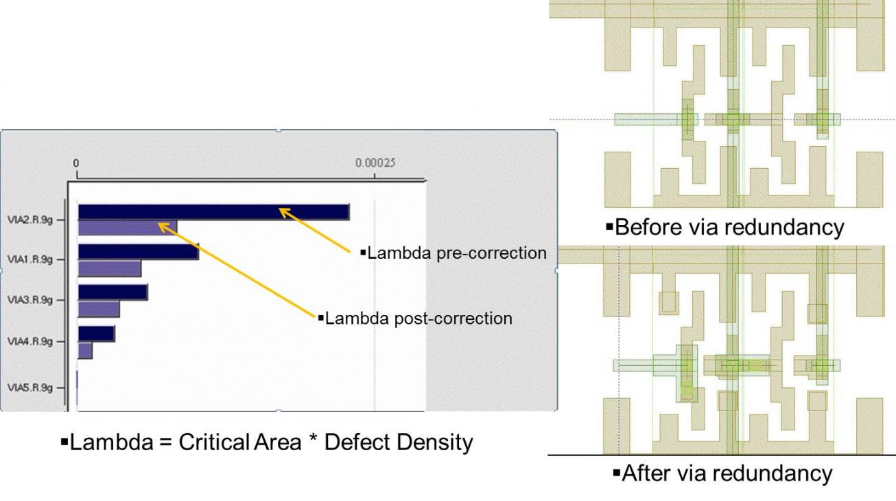
Running CAA through digital blocks revealed that the use of single vias had a big impact on yield, given the defect density values of the manufacturing process. Optimizing via redundancy resulted in a significant improvement (Figure 1). Using this data, CSR were able to modify their place and route (P&R) setups to minimize the use of single vias.

Fig 1. Via redundancy optimization provided a significant improvement in yield.
Using LFD analysis allowed CSR to optimize its layout style to avoid potential lithography issues such as gate corner rounding. As shown in Figure 2, the OD contour variation can cause width deltas and the poly contour can cause length deltas that result in unacceptable gate rounding. With LFD analysis identifying these potential issues early in the design flow, the layout guidelines can be improved to adjust poly to OD spacings, and avoid these effects for sensitive analog circuitry.
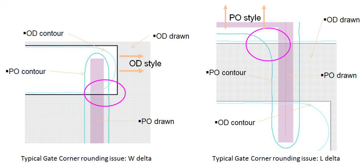
Fig 2. LFD analysis allowed CSR to identify lithography “hotspots” during the design process.
CSR used the CMP analysis along with the “smart” filling techniques of the DFM tool to analyze the thickness and density before and after fill is applied, and achieve a tighter fill distribution (Figure 3). Using these two DFM techniques in tandem enabled CSR to ensure that density and planarity issues were addressed using the appropriate parameters to reflect silicon behavior.
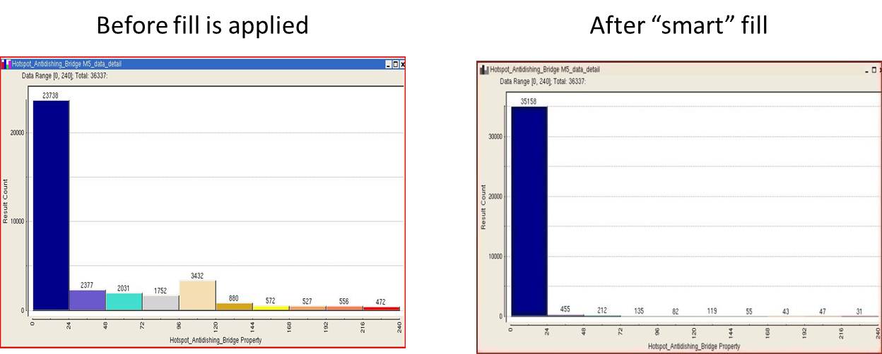
Fig. 3 Using sophisticated fill algorithms in combination with CMP analysis, CSR obtained a tighter fill distribution and a flatter design.
By engaging wholeheartedly in the process, CSR was able to define and apply the critical success factors of the DFM process—first, to understand the impact of the effects addressed by DFM technology and implement design guidelines to minimize their occurrence through careful design, and second, to quickly and efficiently identify and fix any occurrences once the design is underway. In turn, these results had a direct impact on product success. Not only did they achieve yield earlier than planned, but the product performance exceeded expectations. CSR’s proactive approach to DFM implementation substantially reduced their manufacturing risk while improving their competitive position in the market. In addition, their improved design flow and layout style optimizations not only allowed them to achieve their specific target in this project, but increased their chances of success with future designs as well.
This article is based on a joint presentation by Mark Redfordof Cambridge Silicon Radio and Jean-Marie Brunetof Mentor Graphics at the TSMC Open Innovation Platform Ecosystem Forum. View the entire presentation on the TSMC website.


Comments
0 Replies to “DFM Provides Proven Value”
You must register or log in to view/post comments.