The semiconductor industry has built decades of success on hyper-integration to increase functionality and performance while also reducing system cost. But the standard way to do this, to jam more and more functionality onto a single die, breaks down when some of the functions you want to integrate are built in different processes. This is why 3DICs – integration of multiple die in 3D stacks and on interposers – have become popular. One currently popular application combines high bandwidth memory side-by-side with processors, allowing for higher-bandwidth communication through low-impedance / highly-parallel connections directly between DRAM stacks and main memory.
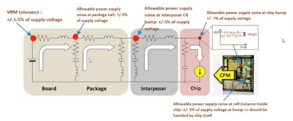
Naturally with each design innovation like this come new design problems. One of these is managing power integrity in these systems all the way out to the package and board level. Normally we think of power integrity analysis and power distribution network (PDN) design as something that can be managed chip by chip, forgetting that this is possible thanks to high impedance between packages, and high chip operating frequencies minimizing inter-chip impact on on-chip power noise. But now we have a range of impedances with low resonant frequencies at the board level (MHz), mid-range at the interposer/TSV level (100s of MHz) and high range (GHz) at the chip level, implying a wide span of potential impact on power integrity. Even where board-level frequencies may still be ignored, those mid-range frequencies cannot.
As a result, it is no longer effective to look at each chip in isolation. Power integrity analysis must look at minimum at the whole 3DIC in package objective. Ansys recently hosted a webinar where they talk in particular about this range of power integrity analysis. There are two major components to this kind of analysis – one is to build an accurate power model for the whole 3DIC device which you can use in detailed transient and AC Spice analysis and the other is to ensure that your models effectively reflect usage across a very wide response range, potentially from board/package level (MHz) up to chip-level (GHz).
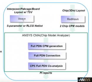
Building an accurate power model has several components. Analysis for a chip/die is already well understood and can be implemented through RedHawk or Totem (for analog designs). RedHawk is also recommended for extraction on the interposer; this is really just another semiconductor device supported by foundry tech files, and extraction here is a task well within RedHawk capabilities. Ansys recommends that extraction for TSVs be handled by SIwave / HFSS. Together these can be combined into a system chip power model (CPM) which you can use for detailed transient and AC analysis in the Ansys Chip Model Analyzer (CMA).
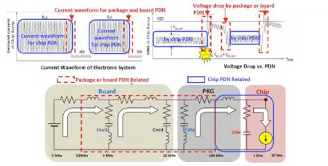
In the second stage of this analysis it is important to ensure that the CPM models reflect the wide response range inherent to the total system. Here, in chip level analysis, you may look at tens of nanoseconds of activity (blue sections above). But at more widely-separated intervals, discontinuous events will happen causing potentially larger power transitions, as a result of perhaps transition from functional activity to an idle mode on another chip in the 3DIC package or even on another device on the board (red sections above).
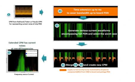
It would be impractical to consider an accurate analysis at the nanosecond level across a microsecond range. Instead CMA provides you with tools to construct a representative power noise frequency spectrum based on a chip-level high-frequency response and lower frequency input which can be generated through a variety of methods to reflect interposer/TSV and package/board response to these discontinuities. These can then be merged to generate a new CPM more accurately mirroring the full range of response.
Methods you can use to model these longer cycle-time events include envelope profiles over long time-frames, for example derived from PowerArtist profiles or through manually-specified profiles (perhaps to reflect on-board sensor switching) or through impedance-aware random noise generation based on the PDN for the 3DIC and perhaps the board.
Fully optimizing the system-level PDN has become even more critical task given these 3DIC devices with their range of resonant frequencies from the chip down to the board level. What is clear is that this now requires a broader analysis. You can request a link to the webinar HERE.
Share this post via:


Comments
There are no comments yet.
You must register or log in to view/post comments.