![]()
It was nice to be at a live conference again. DesignCon was held at the Santa Clara Convention Center, my favorite location, which to me there was a back to normal crowd. The sessions I attended were full and the show floor was busy. Masks and vaccinations were not required, maybe that was it. Or there was a pent-up demand to get back engaged with the semiconductor ecosystem? Either way it was a great conference, absolutely.
SemiWiki stalworth companies Cadence, Ansys, Siemens, and Samtec, were all there. We will have more coverage of their talks over the next week or two. SemiWiki newcomer Xpeedic was there and we will be covering their new announcement as well.
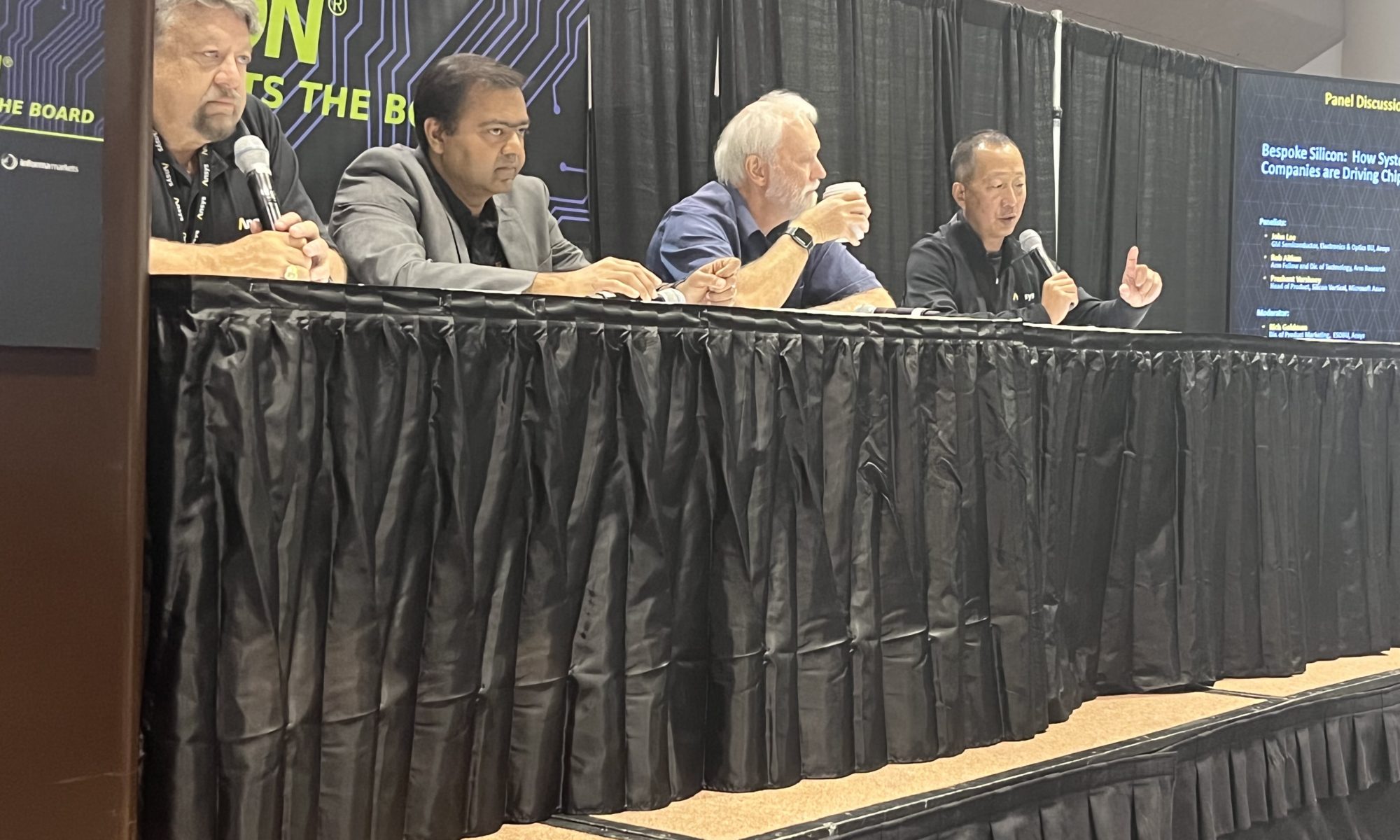
The first panel I attended in the Chip Head Theater was titled Bespoke Silicon: How System Companies are Driving Chip Design. The panelists were John Lee, GM Semiconductor, Electronics, Optics BU, Ansys. Rob Aitken, Arm Fellow and Director of Technology, Arm Research. Prashant Varshney, Head of Product, Silicon Vertical, Microsoft Azure.
This panel was set up to explore the trend of system/software companies deciding they need semiconductor solutions that cannot be bought off the shelf. Some prominent examples of this are Meta, Amazon, Microsoft, and Google who are all defining and designing their own chips. An understanding of what is driving this market trend also gives insights on how it impacts the technical demands on Ansys’ simulation/analysis products.
Why are these companies doing this? The background enabler is, of course, the internet and the pervasive digitalization of society and the economy. But more specifically, it is a confluence of advances in AI/ML algorithms together with semiconductor systems that have become big and complex and capable enough to actually move the needle for an entire business division. Take, for example, Meta’s vision for a VR-enabled future: it all depends critically on the technical capability of the optical headset as well as the power of the AI algorithms driving it – which itself requires a lot of silicon to execute.
Microsoft’s gaming division is only competitive to the degree that its Xbox can stay at the cutting edge of graphic processing. Amazon Web Services finds its costs structure is tied to the price, performance and power profile of the CPUs they use to power their data centers. So they developed their proprietary Graviton2 microprocessor in collaboration with Arm. There are very interesting business dynamics resulting from this that the panel explored.
At the lower, technical level this evolution is driven on the one hand by advances in AI/ML techniques, and on the other hand by advances in integration density with 3D-IC that have accelerated past reliance on just Moore’s Law. We see the latest HPC products from AMD and Nvidia and Intel are all multi-die chiplet systems. The recent industry collaboration on the release of the UCIe spec indicates how seriously these companies take the 3D-IC revolution as an enabler for the systems they want to build. Not to mention that just AI/ML algorithms are driving a leap in design sizes all on their own – see the wafer-scale engine from Cerebras which is explicitly targeted at ML training.
What this means from the Ansys point of view is that they are being called on to analyze increasingly large and complex multi-die systems. That is where the analysis/signoff market is going. However, the technical challenge extends well beyond simple massive capacity (which makes a cloud strategy a must-have for EDA tools). Even more challenging is the emergence of new physical effects that need to be simulated. So, the 3D-IC problem is not just quantitatively bigger, it is also qualitatively different. We call this the multiphysics challenge of 3D-IC.
The primary new physics is thermal analysis since heat dissipation is often the #1 limiting factor on these advanced designs (part of Cerebras’ secret sauce is how they manage to cool their ~15kW wafer). Of course, thermal analysis is not new but it is to most chip designers. It is an example of how chip, package, and PCB design is collapsing into a single design problem. Furthermore, thermal analysis screams out for a computational fluid dynamics simulation engine to model how the air flow and heatsink interact to set boundary conditions for the 3D-IC module. That’s another modeling physics pulled into the mix. And then there are the mechanical stress/warpage issues from having differential thermal expansion in various parts of the 3D-IC stack. Add a mechanical modeling engine to the mix.
One last example of new physics being jammed into the 3D-IC design problem space: electromagnetic analysis of high-speed signals. You see, what makes a 3D-IC integration fundamentally different from just placing two packaged chip next to each other on a PCB is that the inter-chip communication is very low-power and very high-bandwidth. If that can be done, then we can minimize the power/performance cost of going off-chip. But these interconnect traces absolutely require electromagnetic simulation for interference and coupling. How many digital designers are familiar with EM simulation?
Bottom line: The manufacturing process allows us to produce very fine-grain electrical integration of multiple chips. But the success of this market, which is driven in large part by bespoke silicon projects, is gated by the ability of designers to model, simulate, and verify the electrothermal interactions. I believe that is where the true bottleneck to adoption lies, and something Ansys tools are uniquely positioned to alleviate.
Also read:
Webinar Series: Learn the Foundation of Computational Electromagnetics
5G and Aircraft Safety: Simulation is Key to Ensuring Passenger Safety – Part 4
The Clash Between 5G and Airline Safety
Share this post via:


Comments
3 Replies to “Bespoke Silicon is Coming, Absolutely!”
You must register or log in to view/post comments.