Design verification (DV) is still one of the biggest challenges in the ASIC based product world. In last two decades, we have seen many changes in terms of HVLs and methodologies used for design verification. System Verilog is the most popular HVL these days and UVM is the most popular verification methodology.
Even after such an advancement in HVLs and DV methodologies, quality of actual Design Verification is still largely dependent on DV engineer’s verification skills. Due to human intervention, there are chances of design bugs escape in ultimate design. Such design bugs, fall in critical bug category, leads to chip respin which can be very expensive and above all affects the “time to market” of the product which is very critical for a product company.
To avoid such possible design bug escapes and to minimize the risk, chip design companies adopt different tools in addition to actual EDA simulation tools used for verification. This includes formal verification tools, emulation tools and more. The key goal is same and that is to make sure final design that is taped out is design bug free.
Sometimes, Certitude, a tool from EDA tool company Synopsys, is used to measure verification environment strength. The fundamental usage of this tool is to catch DV environment holes that can lead to design bug escape. This paper talks about how the Certitude tool works, how can it help in catching DV environment gaps, it’s pros and cons based on our own experience, where it is used on a complex mix signal ASIC design.
How Certitude Works?
Certitude introduces bugs in specified RTL design modules which are known as “Faults”. It then runs specified (in certitude_testcases.cer) tests using existing verification environment (VE) and checks whether the VE detects the injected fault or not. At least one test is expected to fail for one fault at time due to one or more failing symptoms mentioned below,
- Data checker failure that includes data integrity check OR status check
- SystemVerilog Assertion failures
- Simulation timeout reached.
Certitude mainly divides “Faults” into few class categories. But the most important fault classes that should be exercised and analyzed are as below.
Top Outputs Connectivity:
This category of fault inserts faults on the output signals of top design module (specified in certitude_config.cer).
For an output port of a top module, Certitude updates RTL design by injecting StuckAt1, Stuckat0 and Negated faults. This means actual output port is driven by “1”, “0” OR “inverted” value considering the fault.
See in below top module of a design, for an output port at line 16, certitude injects three different faults,
Top Module of designs specified.
OutputPortStuckAt0 fault (Fault ID 691)
As shown in below snippet, actual output port is commented and internally driven to “0” by tool.
OutputPortStuckAt1 fault (Fault ID 692)
As shown in below snippet, actual output port is commented and internally driven to “1” by tool.
OutputPortNegated fault (Fault ID 693)
As shown in below snippet, actual output port is commented and internally driven to inverted value by tool.
ResetConditionTrue:
This fault class considers reset related signals, which are used to set internal signals, status, and error signals to their Init (PowerOnReset) values.
Example, in below snippet, this category of fault injects three different faults for line 67.
ConditionFalse :
It replaces line 67 with, if(1’b0) begin
ConditionTrue:
It replaces line 67 with, if(1’b1) begin
NegatedCondition:
It replaces line 67 with, if (!(i_async_rst_x) begin
InternalConnectivity:
This fault class considers signals to inject faults to the input of design sub modules.
Below snippet shows a submodule is instantiated in a module and tool has identified 3 faults for port connection at line 503.
The faults are,
InputPortConnectionStuckAt0 (Fault ID 1100)
It replaces line 503 with,
.i_ch1**_x (‘h0) begin
InputPortConnectionStuckAt1 (Fault ID 1101)
It replaces line 503 with,
.i_ch1**_x (‘h1) begin
InputPortConnectionNegated (Fault ID 1102)
It replaces line 503 with,
.i_ch1**_x (~(ch1_**_x[27:0])) begin
Brief on Certitudes Phases:
Certitude runs in the phases listed below. There are options to selectively run one or all pf these phases.
Model Phase:
Certitude analyzes the RTL design and collects all required details about design modules to consider, their outputs, inputs and wires to be considered for different types of faults insertion. This phase finds all possible faults to be considered to exercise design in next phases. Design modules to consider for certitude run can be added in certitude_hdl_files.cer
Activate Phase:
Before starting this phase, one needs create the test suite (tests that DV engineers think can effectively exercise the design modules), which tool will use to exercise the selected RTL design modules. Certitude runs the regression using this test suite and checks that signals on which certitude is going to insert the faults toggle or not. This mean it qualifies the test suite against faults to be inserted. If the fault related signals toggles for a test, then that test is considered as qualified test for that fault and is considered in next detect phase.
Based on the report out of this phase, one needs to update the test suite and run this phase again multiple times to identify more qualifying tests for all “Non Activated” faults. As a final result of this phase, we have test suite that qualifies all faults that tool has identified. There are options to run this phase incrementally so that for each iteration it only considers newly added test to qualify “Non Activated” faults.
Detect Phase:
Certitude injects faults on each qualified signal one by one and runs the regression. At end of the regression, it provides us the summary report how many faults once injected are detected by verification environment. The expectation is at least one test to fail for each fault. The report gives details as,
Detected faults:
Details on all the faults which are detected by the existing verification environment when certitude insert the faults. This number represents faults for which we have some failures. VE can detect design issue for these faults.
Non-detected faults:
Details about faults which are not detected by the existing verification environment when certitude insert the faults. This means, for these faults, none of the test failed. It means VE missed to catch the design bug inserted for all such non-detected faults.
Non-Propagated faults:
These are the faults which though activated, does not change the ultimate design simulation result. This means, final output remains the same with and without the fault.
This can happen when fault propagated the effect up to certain hierarchy but not all the way that enables change in final behavior.
Looking at detect phase report, one needs to analyze the Non-detected and Non-propagated faults. The DV engineer has to look at each fault and decides why it remained Non Detected or Non propagated based on the reference specs. Corrective actions can be taken based on analysis and that includes,
- New test needs to be added in the existing test suite provided to certitude. This can be an existing test OR to be created brand new.
- There are chances that some faults may result in some illegal scenario considering design reference specs. DV engineer can check with the designer for such fault and can decide to exclude it. There are options to disable specific fault(s) once required approval is received from concern person.
- We may end up updating existing checkers to catch such faults.
In case we update any assertion or checker, which is considered as DV update, we have to run Model + Activate + Detect phase again from scratch. If it is just an addition to the test suite then we can just run incremental Activate + Detect phase. This will not exercise existing database for faults already detected.
Below are some basic examples of possible scenarios which certitude can help to catch. We can say them as “DV holes or DV gaps”.
Address flip for memory:
If Memory controller’s output address bits are swapped due to fault insertion for both write and read accesses, then it won’t be detected using normal write and read operations.
To detect this, test with front-door write and backdoor read scenario has to be present in DV test suites. If this test scenario is not present, then Certitude’s “OutputPortNegated” fault remains undetected. Certitude can help to identify such faults if any.
Assertion at sub-module hierarchy:
If SV assertion is written using sub-module’s I/O ports where Certitude inserts faults (StuckAt-1, StuckAt-0, Negated fault), then such faults remains undetected. This is because assertion uses same faulty value to predict/check design behavior.
To catch such faults, assertion has to be written using higher-level module’s port or using some glue logic that derives final values to be driven at the submodule’s port boundary. For example, such logic can include data bus writes OR read requests decoding to derive final control signals to use in assertion rather than using sub module’s i/o ports.
Assertion that checks 1’b1 OR 1’b0 on event:
If SV assertions are coded to check that value on some port is driven 1’b1 OR 1’b0 on some condition and if Certitude inserts faults (StuckAt0 OR StuckAt1) that matches assertion expectation, then it won’t result in any failure. DV engineers can find such coding issues “always PASS” using Certitude that may leads to some interesting scenarios.
Reports and details each report provides:
Below snippets depict certitude results report after the detect phase. Tool allows access to such reports while detect phase is ongoing without affecting simulations running.
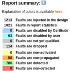
Report Summary:
Below snippet gives overall status of the detect phase.
Report Summary:
Below snippet gives overall status of the detect phase.
Where,
Faults Disabled By Certitude is for faults disabled by certitude based on configuration option settings.
Faults Disabled by User is for user disabled faults based on analysis or discussion with designer.
Faults Dropped are faults that Certitude drops if it is dependent on some other non-detected or non-propagated fault in the same area. For example, if case statement is not detected then tool drops faults on all statements under it
Per Fault Class Summary for a design module:
It shows details related to the faults exercised during detect phase based per Fault Class of a module. So far, this paper has talked about top 3 Fault Class types and they are the one DV engineers should analyze with highest priority compare to others. Reports shows how many faults are detected, non-detected, non-propagated etc for a design module.
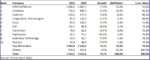
Per Design Modules overall status:
Below snippet shows module-based fault classification. Each module participating in Certitude run and their faults status.
The runtime of the detect phase mainly depends on,
- Number of tests added in Certitude test suite to activate each fault. It is preferred that user identifies the key tests in such a manner which can hit maximum logic in the design. This will help to run a smaller number of tests thus saving on simulation license as well as certitude run time
- Runtime of each test added. Longer the simulation runtime result in increases the detect phase run time
- Number of faults to be exercised. Mode design modules means more faults to exercise and hence more tests required to hit related functional scenarios.
Summary of using Certitude in a project:
- Helps in identifying corner cases which are hard to think about.
- Design module selection and other options allow Certitude to run effectively on key design modules and help to gain confidence on Design Verification done
- It is advisable to run Certitude in the later stage of a project, when most of the DV work is done and once thorough design verification is complete, but this affects the project deadline.
- Some faults are not legal with respect to design spec but still if they fall in Non-Detected or Non-Activated category, one has to spend time closing them, which is time consuming or “Return over efforts” may not add much value.
- Some faults may not lead to use case scenarios of final product but still one may end up spending time to close them.
- Depending of design complexity, tool identifies large number of faults and to run them using certitude is time consuming and needs large number of simulation licenses. This adds an additional cost to the project.
Conclusion:
As described, based on design complexity, third party proven design IPs vs key custom design blocks used in an SoC, one can go with Certitude tool and run it on entire design or on selected design modules to gain more confidence on quality of the design verification done on those design modules. Using this tool, one may or may not find any bugs in design or DV gaps based on how thoroughly the DV is done but it can surely help in gaining DV confidence. Sometimes it leads to uncover some corner case scenarios, which are hard to think about and are missed to cover in verification plan. Based on design specs and use case scenarios, DV engineers can decide on whether to add those scenarios or can get waiver from design leads to drop them.
To know more please see the Synopsys webinar or contact our experts.
Authors-
Manzil Shah – Technical Manager, eInfochips-An Arrow Company
Bipin Patel – Member Technical Staff – (Level 2), eInfochips-An Arrow Company
Vishal Mistry – Member Technical Staff – (Level 2), eInfochips-An Arrow Company
Shashank Mistry – Senior Engineer – (Level 2), eInfochips-An Arrow Company
Ronak Bhatt – Engineer, eInfochips-An Arrow Company
Also read:
Understanding BLE Beacons and their Applications
Digital Filters for Audio Equalizer Design
Sign Off Design Challenges at Cutting Edge Technologies
Techniques to Reduce Timing Violations using Clock Tree Optimizations in Synopsys IC Compiler II