I recently posted an insightful article [1] published in 2013 on the cost of 3D NAND Flash by Dr. Andrew Walker, which has since received over 10,000 views on LinkedIn. The highlight was the plot of cost vs. the number of layers showing a minimum cost for some layer number, dependent on the etch sidewall angle. In this article, the same underlying principles are used to calculate the effective 2D design rule for the 3D NAND array as well as to find the maximum density, both of which are strongly dependent on the sidewall angle of the holes etched through the multilayer stack. A previous article of mine focused on initial estimates of 2D vs. 3D wafer cost [2], but here we will go directly to the impact of 3D processing on the effective 2D density.
Model of 3D NAND cell
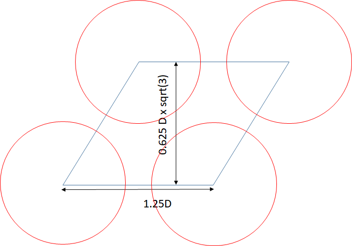
The 3D NAND cell has a typical arrangement as shown in Figure 1. The charge storage areas are circular rings containing at least a nitride layer sandwiched between two oxide layers. The rings encircle a silicon channel, typically also ring-shaped. The circular hole structures are taken to be located on a hexagonal close-packed lattice. If we take the minimum distance between holes to be equal to 1/4 the hole diameter [3], the density will be 2/sqrt(3) ~ 1.155 times that of the case where the same diameter holes are placed on a square lattice with the same minimum distance between holes. This proportionality will help in determining the equivalent 2D design rule later, i.e., the design rule of the 2D planar NAND array with the same density (assuming one bit per cell).

Figure 1. 3D NAND Flash unit cell.
3D NAND Hole Widening
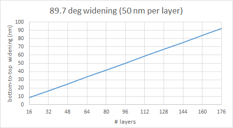
The holes penetrating the layers of the 3D NAND stack are ideally with vertical sidewalls. Realistically, it deviates by a fraction of a degree from normal [4]. As a result, the bottom diameter of the hole will be smaller than the top diameter. It is the top diameter that therefore determines the cell pitch. The widening of the hole diameter from the bottom to the top can therefore be given by:
Top diameter – bottom diameter = cot(sidewall angle) * # layers * layer height.
The top diameter is used to determine the equivalent 2D design rule (E2DDR):
1.25^2 * sqrt(3)/2 * (top diameter)^2 = # layers * 4 * (E2DDR)^2, or
E2DDR ~ 0.58 * top diameter/sqrt(# layers)
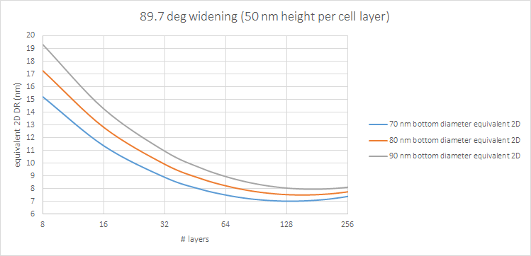
This allows us to predict a maximum density or minimum 2D equivalent design rule for some number of layers, at a given sidewall angle. We can still expect the equivalent 2D design rule to reach 10 nm.


Figure 2. Top: Widening of diameter as stack height increases with number of layers. Bottom: Equivalent 2D design rule vs. number of cell layers, for different bottom diameters, at a sidewall taper angle of 89.7 deg. (visually estimated for Samsung’s 92-layer case from IWAPS 2019 presentation by J. Choe [4]).
Note that the maximum density or minimum equivalent design rule occurs for a smaller number of layers for a smaller diameter. This means taller holes would eventually need to be built up from stacking multilayers supporting shorter holes, with alignment required. It is a vertical analogy to the Litho-Etch-Litho-Etch… multipatterning used by foundries [5]. This is already a common practice among 3D NAND manufacturers [4], with only Samsung holding out so far, but considering it for seventh-generation V-NAND [6].
References
[1] A. J. Walker, IEEE Trans. Semicon. Mfg. 26, 619 (2013).
[2] F. Chen, Toshiba’s Cost Model for 3D NAND: https://www.linkedin.com/pulse/toshibas-cost-model-3d-nand-frederick-chen, also https://semiwiki.com/semiconductor-manufacturers/291971-toshiba-cost-model-for-3d-nand/
[3] A. Tilson and M. Strauss, Intl. Symp. Phys. & Failure Analysis Integ. Circ., 2018.
[4] Some figures for measurement are provided for example in J. Choe’s IWAPS 2019 presentation “Technology Views on 3D NAND Flash: Current and Future.” http://www.chipmanufacturing.org/1-A2-Short%20version%20for%20Publish_IWAPS%202019_Jeongdong%20Choe_TechInsights_3D%20NAND_F_s.pdf
[5] J. Huckabay et al., Proc. SPIE 6349, 634910 (2006).
[6] https://en.yna.co.kr/view/AEN20201201006900320
Share this post via:


Solving the EDA tool fragmentation crisis