
SoC integration offers huge benefits through reduced chip count in finished systems, higher performance, improved reliability, etc. A single die can contain billions of transistors, with multiple processors and countless subsystems all working together. The result of this has been rapid growth of semiconductor content in many old and new products, including automotive, networking, telecommunications, medical, mobile, entertainment, etc. While higher levels of integration are largely beneficial, there are new challenges with system level integration, debug and verification. Embedded Analytics will play an important role in implementing and verifying these large and complex systems.
Many SoCs have large numbers of blocks and subsystems connected through on-chip bus or network interfaces. They use on-chip memory and registers and incorporate complex software running application code. In previous generations system level observation and debug were challenging but made possible through what were previously external connections or in-circuit emulators (ICE). Modern SoCs require a completely new approach to understand dynamic system operation with sufficient visibility and control to make sense of what is occurring during operation.
Siemens EDA writes about this in a white paper called “Embedded Analytics – A platform approach”. They cite the causes of increased design complexity leading to increased difficulty in design, optimization, verification and lifecycle management.
First on their list is multi-source IP, where one SoC will contain IP from numerous sources, both internal and external. These IP elements can include heterogenous processors, interfaces, and a host of other kinds of blocks. Next comes the software for each of these processors. The software could be algorithmic or for managing chip operations or security. Each of these software packages in turn will probably be built on a software stack.
Complexity in these SoCs can come from hardware and software interactions. The Siemens white paper correctly points out that often the kinds of problems caused by these interactions are non-deterministic and efforts to observe them can make them disappear or change behavior. The cost of system level validation can cost tens of millions of dollars. Functional validation needs to start early in the design process through to system installation. System level interactions need to be examined using simulation, emulation, prototyping and in finished systems. Even after product shipment, software updates can cause system level issues that will need to be investigated.
By now it is clear that system level visibility into hardware and software is necessary. Without enough detail it may be difficult to pinpoint problems. On the other hand, too much data can also be an issue. The white paper points out that a truly effective observation and data gathering system for SoCs needs to have sophisticated control over what data is collected and when.
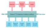
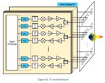
Siemens EDA has developed the Tessent Embedded Analytics platform to allow system designers to wrap their hands around the problems relating to system level real time observation and analysis. There are several pieces to this platform, allowing it to be integrated with the target SoC and then be used to collect and interpret data on system operation.
Tessent Embedded Analytics has an IP subsystem that is integrated into the target SoC. This IP is easily parameterized to make integration efficient and easy. There is also a hierarchical message passing fabric used to transfer the collected data efficiently with minimal added silicon overhead. The message passing fabric can handle local or cross-chip data transfers and is separate from the mission mode interconnect.
To help filter the data collected there are programmable filters, counters and matchers that enable smart and configurable data filtering and event triggering in real time at the frequency of the SoC. There are secure data links for collecting data and interacting with the outside world. Tessent Embedded Analytics contains a software interface layer that communicates between the application layers and the analytics IP.
The Tessent Embedded Analytics platform includes the tools to create applications that interact with its IP components to enable sophisticated monitoring of the SoC. There is a software development kit (Embedded SDK) that lets user developed applications configure, control and process the analytics data. The Configuration API, Data API and Verification API are available for use in either the Tessent Embedded Anaytics IDE or 3rd party IDE environments through plugins.
The Siemens white paper describes in more detail how the entire process works and how it can support prototyping through FPGAs or emulators, as well as in-system silicon. Without an embedded analytics platform, system designers face an almost intractable problem when it comes to verifying and optimizing present day SoCs. Siemens seems to appreciate that while an embedded analytics platform must be comprehensive, it must not require excess silicon resource or interfere with system operation. The full white paper is worth reading to gain a better understanding of how Siemens EDA has assembled a powerful solution for these difficult challenges. The white paper is available on the Siemens EDA website.
Also Read:
Siemens EDA Updates, Completes Its Hardware-Assisted Verification Portfolio
Formal for Post-Silicon Bug Hunting? Makes perfect sense
Library Characterization: A Siemens Cloud Solution using AWS


