Semiwiki EDA Webinar 800x100

How PCI Express 6.0 Can Enhance Bandwidth-Hungry High-Performance Computing SoCs

How PCI Express 6.0 Can Enhance Bandwidth-Hungry High-Performance Computing SoCs
by gruggles on 04-12-2021 at 2:00 pm

How PCI Express 6.0 Can Enhance Bandwidth Hungry High Performance Computing SoCs

What do genome sequencing, engineering modeling and simulation, and big data analytics have in common? They’re all bandwidth-hungry applications with complex data workloads. High-performance computing (HPC) systems deliver the parallel processing capabilities to generate detailed and valuable insights from these applications. To break through any bandwidth limitations, HPC SoCs need the fast data transfer and low latency that high-speed interfaces like PCI Express® (PCIe®) provide. With each new generation of PCIe delivering double the bandwidth of its predecessor, the latest iteration, PCIe 6.0, promises to be a boon for compute-intensive applications.

The HPC solutions that transform high volumes of data into valuable knowledge can be deployed in the cloud or on on-site data centers. Regardless, they demand compute, networking, and storage technologies with high performance and low latency, as well as artificial intelligence (AI) prowess. PCIe 6.0, which is expected to be released sometime this year, is expected to help solve the bandwidth limitations that HPC SoCs are constantly facing. The I/O bus specification will provide:

  • An increased data transfer rate of 64 GT/s per pin, compared to 32 GT/s per pin for PCIe 5.0
  • Power efficiency via a new low-power state
  • Cost-effective performance
  • Backwards compatibility to previous generations

Faster data transfer via PCIe 6.0 will result in faster computations for HPC, as well as cloud computing and AI applications. For example, as an AI algorithm is being trained, data needs to move back and forth quickly across multiple processors. PCIe 6.0 will remove the bottlenecks to allow a fast data flow for a more rapid training process. At the moment, the HPC landscape is dominated by hyperscale data centers. Given their disaggregated computing structure, hyperscale data centers currently provide the most powerful HPC capabilities for applications like AI engines. PCIe 6.0 will be beneficial by supporting more efficient disaggregated computing.

Another emerging application for PCIe 6.0 is storage, namely solid-state drives (SSD) used in data centers. Technology advances in SSD manufacturing—including stacked die—have increased storage capacity. At the same time, this has pushed the limits of 4-lane PCIe form factors. PCIe 6.0 will open the doors to the bandwidth and fast data transfer needed to take full advantage of the increased storage capacity.

New Architecture Brings New Challenges

PCIe 6.0 does come with a new architecture, moving from the non-return-to-zero (NRZ) structure with two logic levels of previous generations to Pulse Amplitude Modulation with four levels (PAM-4). PAM-4 encoding brings the increased data transfer rate and bandwidth. The latest generation also introduces forward error correction (FEC) to address raw bit error rate (BER) challenges that result from the new architecture. FEC traditionally introduces latency; however, PCI-SIG has defined a “lightweight FEC” with retry buffers and cyclic redundancy check (CRC) to maintain low latency. Another change in this iteration is the move to FLIT (flow control unit) mode, which also supports low latency and high efficiency.

PCIe 6.0 moves from the NRZ structure to PAM-4 for faster data transfer and higher bandwidth

Transitioning to this new architecture from earlier PCIe generations will involve some design considerations. For example, the receiver architecture for the PAM-4 PHY is based on an analog-to-digital converter, which calls for optimization of analog and digital equalization to achieve the optimal power efficiency regardless of the channel. Given the massive data pipe involved—potentially up to 1TB per second of data being moved in each direction—proper management of this data is critical. Another consideration relates to testbench development for verification, which ideally should be as efficient a process as possible while also accounting for factors like functional coverage.

Complete IP Solution for PCIe 6.0

Synopsys, which has long been a key contributor to PCI-SIG workgroups, has unveiled a complete IP solution that will allow for early development of PCIe 6.0 SoC designs. Synopsys DesignWare® IP for PCIe 6.0 is built on the silicon-proven DesignWare IP for PCIe 5.0 and supports the latest features of the upcoming new specification. As such, the solution is designed to address the bandwidth, latency, and power-efficiency demands of HPC, AI, and storage SoCs. The solution consists of:

  • The DesignWare Controller for PCIe 6.0, which utilizes a MultiStream architecture consisting of multiple interfaces to provide the lowest latency with maximum throughput for all data transfer sizes. Available in a 1024-bit architecture, the controller allows designers to achieve 64 GT/s x16 bandwidth while closing timing at 1 GHz.
  • The DesignWare PHY for PCIe 6.0, which provides unique, adaptive digital signal processing (DSP) algorithms that optimize analog and digital equalization for maximum power efficiency across backplane, network interface cards, and chip-to-chip channels. With its diagnostic features, the PHY enables near-zero link downtime. Its placement-aware architecture minimizes package crosstalk and allows dense SoC integration for x16 links.
  • Verification IP, which uses a native SystemVerilog/UVM architecture that can be integrated, configured, and customized with minimal effort to help accelerate testbench development while providing a built-in verification plan, sequences, and functional coverage.

Data Makes the World Go ’Round

It’s a data-driven world, and this will only intensify in the coming years. By 2025, according to IDC estimates, worldwide data will grow to 175 zettabytes, with as much of this data residing in the cloud as in data centers. That’s a 61% compounded annual growth rate from 33 zettabytes in 2018. While PCIe 6.0 early adopters are anticipated to be hyperscalers and other HPC SoC designers, the newest standard promises to eventually gain traction among designers working on edge, mobile, and automotive applications. While leading the shift to PCIe 5.0 with hundreds of design wins, Synopsys is helping designers gain a head-start on PCIe 6.0 designs with a complete PCIe 6.0 IP solution and expertise in the popular high-speed SerDes IP. As bandwidth demands increase, designers of PCIe 6.0-based applications can be well-positioned to keep the data moving.

By Priyank Shukla, Staff Product Marketing Manager, High-Speed SerDes IP, and Gary Ruggles, Sr. Staff Product Marketing Manager; Solutions Group
Also Read:

Why In-Memory Computing Will Disrupt Your AI SoC Development

Using IP Interfaces to Reduce HPC Latency and Accelerate the Cloud

USB 3.2 Helps Deliver on Type-C Connector Performance Potential


eFPGA IP – in Videos

eFPGA IP – in Videos
by Daniel Nenni on 04-12-2021 at 10:00 am

Menta eFPGA IP

eFPGA has been a hot topic on SemiWiki for the past five years and it is still going strong. eFPGA is more descriptively categorized as embedded programmable logic and reconfigurable computing. Whatever you want to call it, eFPGA is an important piece of the computing puzzle, absolutely.

We recently did a series of videos with Menta that is worth seeing as a retrospective of were eFPGA is used today and some hints for tomorrow.

The first one is titled Design Adaptive eFPGA IP:

“In this webinar, we will explain what makes an eFPGA different to a FPGA but also to embedded CPUs/GPUs – and in which cases an eFPGA IP is the way to go. We will then explain what is a design adaptive eFPGA IP and why this adaptiveness is so important when it comes to integrating an eFPGA IP.”

The second one is titled: eFPGA Using Adaptive DSP:

“In this webinar, we will explain why the use of Menta Adaptive Digital Processor (DSP) makes Menta eFPGA different to any other FPGA, embedded CPUs/GPUs or eFPGA. We will then explain why its ease of use, its adaptiveness and its performance are so important when we are looking for the best trade-off between flexibility and PPA to better suit your hardware requirements”

The third one is titled: How to build a secure system over the time using eFPGA IP

“In this webinar we will present the Secure-IC & Menta corporate overview and vision, why eFPGA can be powerful in security, the first results of the collaboration, the joint value proposal summary, and what is coming next for eFPGA IP in secure Element.”

What is the value proposition of eFPGA you ask?

Secret protection: With Menta eFPGA you can wait to deliver your most proprietary technology to end-customers as a field-upgrade, minimizing any opportunity for competitors to reverse engineer your product.

Cost reduction: At higher production volumes, onboard FPGAs quickly become cost prohibitive. With Menta eFPGA you integrate on-board FPGA functionality.

Performance: With Menta eFPGA, sacrifices in board-space, I/O latency, and bandwidth disappear, as you bring those accelerators on-chip, without the limitations/overhead due I/O padcount or chip-to-chip communication interfaces.

Lower power: In a COT FPGA, all the extra to the programmable logic, such as high-speed interfaces, PLL, and controllers consume around half of the power. All our power saving advances lead an algorithm on a Menta eFPGA IP to consume between 10 and 50% of the power of the same algorithm on a FPGA.

Design insurance: Maximizing flexibility requires maximizing process-portability. Menta eFPGA is the only 100% standard-cell based solution and this approach enables rapidly porting your eFPGA to whatever new process geometry/variant you desire, using the same automated, standard EDA flow as for the rest of your SoC. Menta, using our industry gold-standard Synopsys-based implementation flow, enables portability within just weeks.

Security: In today’s global, multi-player design-chain, preserving IP/trade secrets is more critical and challenging than ever. With Menta eFPGA you can wait to deliver your most proprietary technology to end-customers as a field-upgrade, minimizing any opportunity for competitors to reverse engineer your product.

ABOUT MENTA
Menta is a privately held company based in Sophia-Antipolis, France. For ASIC and SoCs designers who need fast, right-the-first time design and fast time to volume, Menta is the proven eFPGA pioneer whose design-adaptive standard cells-based architecture and state-of-the-art tool set provides the highest degree of design customization, best-in-class testability and fastest time-to-volume for SoC design targeting any production node at any foundry. For more information, visit the company website: www.menta-efpga.com


Meeting the Need for Hardware-Assisted Verification

Meeting the Need for Hardware-Assisted Verification
by Lauro Rizzatti on 04-12-2021 at 6:00 am

image001 5

Editor’s Note: Siemens EDA recently introduced a comprehensive hardware-assisted verification system comprised of hardware, software and system verification that streamlines and optimizes verification cycles while helping reduce verification cost. What follows is an edited version of an interview Verification Expert Lauro Rizzatti conducted with Jean-Marie Brunet, senior director of product management and engineering for emulation and prototyping at Siemens EDA.

LR: Siemens EDA introduced a suite of comprehensive and integrated hardware-assisted verification tools. Before we discuss the details of this “Big Launch,” let me ask you a general question to set the stage. What trends do you see in chip design and what is driving those trends?

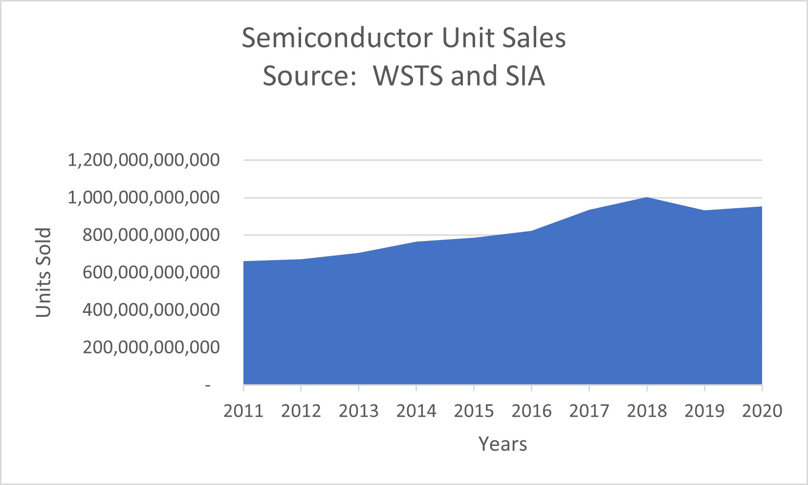
JM: The market trends we see in IC verification and validation are interesting and promising for us. We see that verification costs continue to grow faster than design costs. As software validation costs grow , hardware verification spending overtook register transfer level (RTL) simulation spending in 2018 and this trend continues for the foreseeable future. All market indicators are moving in the direction of the need for more hardware-assisted verification tools, and more spending in this category, which is good news for us.

We see four major markets driving our hardware-assisted verification technology investment.

Number one is networking. Number two is communication with 5G. Number three is computing and storage. Number four is transportation, not only automotive, but any type of transportation.

Consistently, all four vertical markets share the same challenges when designing, verifying, and realizing an IC. The challenges come from the ability to meet power consumption and performance targets.

LR: System-on-Chip (SoC) designs consist of a combination of hardware and software, where software is becoming the dominant contributor. How do you measure success designing such a complex design?

JM: This is an interesting question. The market dynamics driving IC verification are clear. We are moving into an era where software performance defines semiconductor success. It used to be that meeting hardware functional specs defined semiconductor success. While today you still have to meet hardware functional specs, on top of that, you have performance and power targets. The challenge can be met by handling a test environment consisting of lots of workloads, frameworks, and industry benchmarks. Clearly, today’s SoC designs are driven by software performance. That’s the key trend we see.

For any vertical market segment, there is a long list of different workloads or benchmarks that must be executed to certify a design. Looking at artificial intelligence (AI), machine learning ML and deep learning (DL), you have many different types of frameworks or workloads that must be run. The same is true for advanced driver-assisted systems (ADAS) where lots of sensor and raw sensor fusion data must be processed. For the mobile market, we used to see activity within AnTuTu as the main reference. With graphics, we see a lot of Kishonti type of benchmarks. The bottom line is that there is a wide variety of frameworks and benchmarks that have to be run.

For those who paid attention to the announcement by AMD of its third generation EPYC server, the reference to SPECint and SPECfp was captured many times in the slides. Those benchmark references must be run pre-silicon while monitoring the behavior of the design. They are really the references that semiconductor companies use to position their products. They define how products must behave within the context of software workloads.

LR: Let’s move on and discuss your “Big Launch” and the specifics encompassing the launch of the Veloce Suite targeting the verification space. How is software changing the verification process?

JM: The story behind the “Big Launch” is relatively simple –– we identified three reasons driving the need for a complete and integrated suite of hardware-assisted verification tools designed around our Veloce emulation platform.

First, the software environment that we just described in terms of workload requires a massive amount of cycles to run. Billions of cycles are needed for booting operating systems, running benchmarks, and even applications.

Second, it is critical to estimate and measure power and performance while processing these massive workloads. For that you need visibility, accurate analysis and comprehensive debug tools.

And the third aspect is the size and the complexity of the SoC system that now can exceed many billions of gates. You cannot handle such complexity without a hardware-assisted platform.

We launched a suite of products built around our Veloce hardware-assisted verification platform. The first one is Veloce HYCON, our virtual platform to validate software. The second is Veloce Strato+, our new generation of emulator. The third is Veloce Primo, our brand-new enterprise FPGA prototyping engine, and the fourth is Veloce proFPGA, offered through an OEM relationship with ProDesign, to address the desktop FPGA prototyping market.

Based on this offering, we assert not only that the IC verification market needs a complete and integrated solution, but also it needs to approach verification with the context of the right tools for the right tasks. Throughout the verification cycle of an SoC design, different milestones must be met, and these different steps have different needs. Very early on, you need a virtual platform that requires virtual models to process software workloads with a tight integration to hardware emulation to take charge of RTL design blocks. At this stage, it’s all about speed. Eventually, your RTL becomes stable. Now you need to debug your RTL with full design visibility. You need different verification use models. You need scalable design capacity. All of the above needs are offered by an emulator like Veloce Strato+ that allows you to perform power analysis and gate-level emulation. As you approach tape-out, you have a gate-level netlist. Now you have to perform accurate power analysis. Only emulation like Veloce Strato+ can do the job.

We are also introducing a new concept called Emulation Offload from our Veloce Strato+ emulator to our enterprise field programmable gate array (FPGA) prototyping tool, Veloce Primo. The concept here is, early on, you need an emulator that provides accurate and efficient RTL debug. At some point, the design becomes more stable and less buggy, and then you need to verify at a higher speed. At this stage, you want to trade off debug for speed. You can do that by offloading the design from the emulator to the enterprise prototyping tool to accelerate the verification cycle and reduce the cost of verification task.

The last piece of the launch is our desktop FPGA prototyping with Veloce proFPGA, a single-user, smaller footprint type of prototyping tool that sits on the desk or in the lab, with easy bring up and very fast execution.

LR: Could you explain the positioning of the Siemens EDA suite of verification tools against the competition? How are they addressing the challenges you enumerated and why do you think your solution is superior to their offerings?

JM: In the highly competitive market we operate in, there are two critical factors. First is the timing. You have to be first, because when you are first, you define a direction that moves the market forward. That’s what we have accomplished with this launch. The second factor is that you have to offer a complete solution. In the past, we were known only for providing a point tool –– that is, an emulator.

With this launch, we now have all the necessary pieces, well integrated with each other where each tool is the right solution for the right task. This is how we are different from our competitors.

Let’s start with Veloce HYCON, an evolution of the traditional virtual platforms and hybrid emulation offerings. It stands for HYbrid-CONfiguration for the included set of configurable reference platform. Via HYCON, users enjoy an end-to-end software-enabled verification and validation solution that allows them to implement a shift-left strategy by providing a hardware-assisted verification environment where softwre development and validation occurs in parallel with hardware design and verification.

Next is our Strato+ emulation platform. Not all emulators are created equal. The foundation of what we do in Veloce Strato+ sits on three pillars.

The first pillar is the chip. We designed our Crystal chip, essentially a custom-emulator-on-chip. The second is the system hardware architecture. We also completely architect our hardware from the ground up. And the third is the software. We design the chip and the system hardware at the same time we design the software so all three are tightly coupled. When you design a new generation of a tool, you’re looking at what enhancements should be implemented.

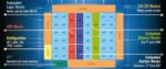
With Veloce Strato+, we realized two types of improvement. The first improvement is in capacity. We implemented an exact 1.5X increase in capacity by starting at the source of the Crystal chip. Here we created on a new 2.5D IC package. We integrated a good portion of the memory components that were previously on the board onto the substrate of the package. With this silicon innovation we were able to free up space on the board. Now instead of installing 16 chips on a board as it is with Veloce Strato, with Veloce Strato+ we have 24 chips – 24 divided by 16 leads to an exact increase of capacity of 1.5X.

The second improvement is in performance. Performance comes from a combination of multiple things, from speed of compilation to speed of execution, all contribute to increase the throughput. To accelerate compilation, we implemented a hierarchical flow. Today, every big design is hierarchical, which extends the benefit to virtually all SoC designs. Regarding run-time execution, some emulator providers talk about clock speed and how quickly the chips are running. That’s one aspect and an important aspect, but it’s not the only aspect. What matters is total throughput or what is known as wall-to-wall execution time. That execution time includes processing on the co-model host, plus the interaction with the system hardware. Clearly, the channel-communication architecture is a critical element to achieve the best results.

Within the system hardware, data travels from point-to-point often via a backplane, another critical component for fast execution. At some point, the design data is mapped to the boards in the emulator. Now, the clock speed of the chip becomes important. When data emerges from the chip, it propagates through the backplane to the communication channel, then to the host. The addition of all the above accounts for the total execution time. It is throughput that matters. The Veloce architecture is tailored to optimize throughput and reduce total execution time. On every step along the way, Veloce offers superior throughput to other emulation alternatives on the market.

And the third improvement is improved design debug efficiency. The Crystal 3+ chip provides 100 percent visibility. This is a fundamental advantage of the Veloce Strato platform and the roadmap for future generations of Veloce, continuing on this path of offering superior debug capability versus FPGA-based emulators.

Regarding prototyping, Veloce Primo enterprise prototyping provides five fundamental advantages.

First is performance. Performance ranges from about seven megahertz (MHz) for very large designs up to 70 to 100 megahertz for smaller single FPGA designs.

Second is scalable capacity from a single FPGA user granularity all the way to 320 FPGAs, providing over 10-billion gates in design capacity, certainly enough capacity to handle extremely large SoC designs.

Third, it has the best probe-based debug capabilities in an enterprise prototyping platform for both in-circuit emulation (ICE) and virtual environments. Full visibility is supported by reconstructing combinational values from register data. Design states can be captured at speeds up to 300 MHz. Root cause detection of hard-to-isolate bugs can be accelerated by exporting the design under test (DUT) and test environment from Veloce Primo to Veloce Strato to enjoy faster recompile-debug turnaround time and a higher level of visibility and control.

The fourth advantage is productivity through the consistency of the emulation-prototype flow making it easy for designers to migrate from emulation into prototype and to return to debug prototypes within that Veloce Strato environment. This consistency delivers the ability to have the same DUT RTL and the same virtual environment functioning in both emulation and prototyping.

And, finally, number five is the lowest total cost of ownership, a key value for Veloce Primo. We are the industry leader in both low power consumption and density as we can fit 80 FPGAs in a single 42U rack. We also deliver lights-out remote management to make the day-to-day operational support of your FPGA prototyping farm very cost effective with job scheduling and monitoring as well.

LR: It sounds like a breakthrough introduction. To conclude, could you summarize the story for our audience?

JM: Sure. A key goal of the launch was to be first. As I said before, when you are first, you’re establishing a direction in the industry. We now have defined a direction, namely, you need a complete and fully integrated solution with the right tool for the right task.

To summarize, we introduced an entire new suite of verification tools, well integrated into a consistent flow. For the first time, we provide a versatile offering in FPGA prototyping from enterprise to desktop levels.

We have delivered on time with confidence based on our emulation roadmap. Compared to our competition, the confidence level of delivering against the roadmap is not the same as ours. Fully funded by Siemens, we are executing on our roadmap. The notion of having all the pieces fully integrated is clearly demonstrated in this launch. The future looks very bright for this type of complete and integrated platform.


Apple’s Cook Paints Himself into an Autonomous Corner

Apple’s Cook Paints Himself into an Autonomous Corner
by Roger C. Lanctot on 04-11-2021 at 10:00 am

Apples Cook Paints Himself into an Autonomous Corner

These days tech journalists and analysts appear confident of one thing. Apple is working on an autonomous car.

There’s a “Garbo Talks” quality to the tea leaf reading around Apple’s autonomous vehicle development efforts. The latest chapter was written with the publication of Kara Swisher’s latest “Sway” podcast episode in which she interviews Apple CEO Tim Cook.

“Is Apple’s Privacy Push Facebook’s Existential Threat?” – https://tinyurl.com/ynauapr9 – “Sway” podcast

Near the end of the episode, which largely focuses on Apple’s App Tracking Transparency initiative, Swisher takes a few shots at unearthing some details regarding Apple’s automotive efforts. She notes the Elon Musk, CEO of Tesla Motors, comment that he had offered his company to Apple for one tenth of its value but couldn’t get a response from Apple. She also astutely notes that Apple famously eschews high priced and high profile acquisitions.

For his part, Cook coyly comments that he has never met Musk, though he admires him and his achievement of establishing and preserving electric vehicle leadership. He then adds:

“The autonomy itself is a core technology in my view. If you sort of step back the in a lot of ways the car is a robot.  An autonomous car is a robot.  There’s lots of things you can do with autonomy.  We’ll see what Apple does.  We investigate so many things internally.  Many of them never see the light of day.  I’m not saying that one will not.”

Swisher: “Would it be in the form of a car or the technology within a car.”

Cook: “I’m not going to answer that question.”

Swisher: “I think it has to be a car. It can’t be just… You’re not Google.” Swisher is referring to Google’s automotive strategy which has included injecting Android operating system software into embedded infotainment systems, enabling Android smartphone mirroring, and Alphabet’s Waymo initiative which is reliant on mass produced vehicles equipped with Waymo-developed hardware and software.

Cook: “We look to integrate hardware, software, and services and find the intersection points of those because we think that’s where the magic occurs.  And so that’s what we love to do.  We love to own the primary technology that’s around that.”

Swisher: “I’m going with car with that if you don’t mind…”

So we know Apple’s autonomous vehicle plans for what they are not rather than for what they are.  Cook won’t say.

From what he has said, though, one might presume that Apple has considered the options and has already eliminated a few. For example:

Might Apple acquire an EV startup or legacy auto maker?  Apple has no history of massive acquisitions of the sort necessary to bring the company more directly and immediately into the automotive industry generally, whether to manufacturer human controlled or autonomous vehicles.  Besides, it is likely that any existing auto maker would have to be reorganized from the inside out to suit Apple’s requirements and vision.

Might Apple license its software for integration into existing mass produced vehicles?  Apple’s Cook appears to be interested in owning the entire hardware-software-services nexus, which would appear to rule out a licensing scheme.  Apple’s Cook is unlikely to be granted sufficient control over the hardware-software-service nexus for him or the licensing partner to be comfortable.

Might Apple create an aftermarket/add-on module for vehicles – to be built in at the factory or sold retail (a la Amazon Echo Auto)?  This seems highly unlikely and a half-assed approach to a market entry.  Once again, Apple’s control over the customer experience would be limited, compromised.  Such strategies and devices have seen limited success.

Like Google, Apple has a foothold in the automotive industry thanks to its CarPlay smartphone mirroring and the adoption of its Siri voice recognition by multiple auto makers.  But reports from multiple media outlets point to the hiring of hundreds of engineers – including many former Tesla executives – all tasked with creating an Apple car of some kind – autonomous or not.

Apple has approximately $200B in cash on hand – precisely the kind of cash pile necessary to sustain an automotive market entry through the expensive process of tooling, hiring, plant building, and vehicle production.  Interest in an Apple car of some kind appears to be robust.

Technically, there is not much new that Apple can bring to the automotive party.  Apple has its own vision of electrical architecture, but nothing particularly revolutionary.  There is general agreement that Apple does not possess groundbreaking battery technology, in spite of speculation to the contrary.

Apple has some patents around sensing technology and experience in AI and augmented and virtual reality – but nothing particularly automotive oriented.  And reports suggest that the performance of Apple’s autonomous test vehicles in California has been unremarkable.

Apple has four assets that might help define a path to market.  Apple has emotional appeal.  Apple has its focus on privacy.  Apple has its “Think different” ethos.  And Apple has a global distribution network and a unique hands-on approach to customer service.

It’s entirely possible that Apple could bring some unconventional one or two-seat vehicles to market, in the manner of Renault’s Twizy two-seater or Daimler’s Smart cars.  These vehicles have found enthusiastic followings, though sales volumes are still well shy of the millions that would be more attractive to mass market auto makers.

There is room for innovation in electric vehicle charging.  Perhaps Apple could find success in swappable batteries where Better Place failed.

The existing excess manufacturing capacity in the automotive industry is equivalent to one-third of current production.  Much of that excess capacity is in the hands of current market leaders in the U.S.  Apple would be an ideal contract manufacturing partner to target the passenger vehicle market now being collectively abandoned by Ford Motor Company, General Motors, and Stellantis in the U.S.  So Apple has the engineering talent, it has an enthusiastic clientele, it has a distribution network, and it has a coy CEO who may be experiencing automotive hesitancy – strange to see in a time of SPAC-happy investors leaping blindly into billion-dollar EV opportunities.

If autonomous operation is the focal point for Apple’s automotive ambitions, one can expect continued vapor lock.  The path to market via robotaxis is muddled and via semi-autonomous mass market vehicles (a la General Motors Super Cruise or Tesla Autopilot) is fraught with regulatory, user experience, and technical challenges.

The final notable Apple car rumor is the 2024 timing for launch.  In the end, the market is ready and waiting for Apple, and Cook.  It seems customers are more interested in an Apple car than is Apple.


Technology Under Your Skin: 3 Challenges of Microchip Implants

Technology Under Your Skin: 3 Challenges of Microchip Implants
by Ahmed Banafa on 04-11-2021 at 6:00 am

Challenges of Microchip Implants

As technology continues to get closer to merge with our bodies, from the smart phones in our hands to the smartwatches on our wrists to earbuds. Now, it’s getting under our skin literally with a tiny microchip. A human microchip implant is typically an identifying integrated circuit device or RFID (Radio-Frequency IDentification) transponder encased in silicate glass and implanted in the body of a human being. This type of subdermal implant usually contains a unique ID number that can be linked to information contained in an external database, such as personal identification, law enforcement, medical history, medications, allergies, and contact information. [6]

In Sweden, thousands have had microchips inserted into their hands. The chips are designed to speed up users’ daily routines and make their lives more convenient — accessing their homes, offices and gyms is as easy as swiping their hands against digital readers. Chips also can be used to store emergency contact details, social media profiles or e-tickets for events and rail journeys. [2]

Advocates of the tiny chips say they’re safe and largely protected from hacking, but scientists are raising privacy concerns around the kind of personal health data that might be stored on the devices. Around the size of a grain of rice, the chips typically are inserted into the skin just above each user’s thumb, using a syringe similar to that used for giving vaccinations. Implanting chips in humans has privacy and security implications that go well beyond cameras in public places, facial recognition, tracking of our locations, our driving habits, our spending histories, and even beyond ownership of your data, which poses great challenges for the acceptance of this technology. [1][2]

To understand the big picture about this technology, you need to know that the use of the chips is an extension of the concept of Internet of Things (IoT), which is a universe of connected things that keep growing by the minute with over 30 billion connected devices at the end of 2020, and 75 billion devices by 2025. Just as the world begins to understand the many benefits of the Internet of Things, but also learns about the ‘dark side’ from ‘smart everything,’ including our connected cities, we are now looking at small chips causing major new privacy challenges. [1][5][7]

Like any new trend, in order for that trend to be accepted and become main stream, it needs to overcome three challenges: Technology, Business, and Society (regulations and laws)

The first challenge is Technology: which is advancing every day and the chips are getting smaller and smarter, in the world of IoT the chips are considered as the first element of a typical IoT system which consists of: Sensors, Networks, Cloud, and Applications. As a sensor, the chip touches upon your hand, your heart, your brain and the rest of your body —literally. This new development is set to give a very different meaning to ‘hacking the body’ or biohacking. While cyber experts continue to worry about protecting critical infrastructure and mitigating security risks that could harm the economy or cause a loss of life, implanted chips also affect health but add in new dimensions to the risks and threats of hacking of sensors as they considered as the weakest link in IoT systems [1]

The second challenge is Business: there are many companies in this field and the opportunities are huge with all aspects of replacing ID in stores, offices, airports, hospitals just to mention few. Also, chips will provide key physical data and further processing of that data in the cloud to deliver business insights, new treatments, and better services — presents a huge opportunity for many players in all types businesses and industries in private and public sectors. [5]

The third challenge is Society: As individuals try to grapple with the privacy and security implications that come with technologies like IoT, big data, public- and private-sector data breaches, social media sharing, GDPR, a new California privacy law CCPA, along with data ownership and “right to be forgotten” provisions, along comes a set of technologies that will become much more personal than your smartphone or cloud storage history, and the tiny chip under your skin is sitting at the top of the list of these technologies, posing new risks and threats. [1]

This challenge can be divided into two tracks: Government regulations like GDPR in EU and recent regulations in the US to ban forced usage of the chip for example, and consumer trust which is built on three pillars; SSP (Security, Safety and Privacy):

Safety is a major concern in using tiny chips inside your body including infection risks, MRI’s use with chips, and corrosion of the chip’s parts.

Security and Privacy concerns deal with stolen identity, risk to human freedom and autonomy to mention few. [6]

This technology is promising and another step towards more convenience and simplifying many of the daily tasks of billions of people around the world, but without solid security, safety and privacy measures applied when using this tiny chip, we will be facing a cybersecurity nightmare with far reaching consequences, in addition to an ethical dilemma in dealing with population who refused to use it is, they will be marginalized when it comes to jobs for instance. According to a recent survey of employees in the United States and Europe, two-thirds of employees believe that in 2035, humans with chips implanted in their bodies will have an unfair advantage in the labor market. One big concern raised by many privacy advocates is the creation of surveillance state tracking individual using this technology. [3]

Too many moving parts to deal with, in this technology, until we answer all questions related to this technology, many people will look at it as another attempt of both governments and businesses to gain access to another piece of data about us and add it to many channels used now in gathering info. using our electronic devices, knowing that by 2030, there will be an average of 15 IoT devices for each person in the US. [7]

Ahmed Banafa, Author the Books:

Secure and Smart Internet of Things (IoT) Using Blockchain and AI

Blockchain Technology and Applications Read more articles at: Prof. Banafa website


Podcast EP15: The Birth of Dynamically Reconfigurable Computing

Podcast EP15: The Birth of Dynamically Reconfigurable Computing
by Daniel Nenni on 04-09-2021 at 10:00 am

Dan and Mike are joined by Geoff Tate, founding CEO of Flex Logix. Geoff has a storied career in semiconductors that includes over ten years at AMD, ending as senior VP, microprocessors and logic. Following AMD, Geoff was founding CEO of Rambus, growing the company from four people to IPO with a $2 billion market cap.

As co-founder and CEO of Flex Logix, Geoff is leading the creation of a new category, dynamically reconfigurable computing. Geoff explains what the impact of this new category is today and in the future. He touches on inference applications as well as others and details what unique technology requirements are needed to make dynamically reconfigurable computing a reality.

The views, thoughts, and opinions expressed in these podcasts belong solely to the speaker, and not to the speaker’s employer, organization, committee or any other group or individual.

Flex Logix


CEO Interview: Kush Gulati of Omni Design Technologies

CEO Interview: Kush Gulati of Omni Design Technologies
by Daniel Nenni on 04-09-2021 at 6:00 am

Kush Gulati

Kush Gulati is the CEO of Omni Design Technologies, a company he co-founded in 2015 to lead a transformation in how high-performance analog IP is developed and integrated into SoCs in advanced process nodes. With a PhD from MIT, he is a renowned expert in data converters, and a serial entrepreneur. His first startup was a detective agency he started when he was in middle school — Omni Design is his fifth business. Kush’s previous startup – Cambridge Analog Technologies – was acquired by Maxim Integrated in 2011 and, after a few years leading the Advanced IP Solutions group at Maxim, he founded Omni Design in 2015. Speaking to Kush, I am immediately struck by his innovative thought process, clear vision of the future of the semiconductor industry and for how Omni Design is enabling highly differentiated SoCs across a wide range of emerging applications, including 5G, wireline and optical communications, automotive/ADAS, AI, and IoT.

Please tell us about Omni Design?

Omni Design was founded to meet an industry need. The world we live in is analog, and virtually all the data processing is digital. So… you need to translate the analog data into digital, process it, and then transform it back to analog to operate in the real world. Technologies such as 5G, autonomous vehicles, optical computing, and image processing are driving exponential growth in the requirements to receive and transmit data at ever-increasing speeds and dynamic range using ever lower energy.

Traditional suppliers of analog-to-digital converters (ADCs) and digital-to-analog converters (DACs) have been selling discrete devices that are incorporated onto a printed circuit board with the rest of the systems. As systems have become both more integrated and more powerful, there is a tremendous and growing industry demand for these ADCs and DACs in the form of embedded IP cores.

Omni Design is helping meet this demand by offering a portfolio of ADCs and DACs at various resolutions (from 6-bits to 14-bits) and sampling rates (5 Mega samples per second to 20+ Giga samples per second) in 28nm and advanced FinFET process technologies.

Omni Design has a tremendously creative team – this is at the very heart of our ability to build complex circuitry that expands the state of the art while simultaneously achieving a very high rate of first silicon success.

What makes Omni Design unique?

First of all, Omni Design has invented techniques that not only improve the power efficiency and the performance of data converters and analog circuits but also those that enable analog designs that are extremely compatible with FinFET design. This makes our products easier to integrate with digital circuits in advanced FinFET processes which is of course key to enabling complex SoCs for applications such as 5G and LiDAR.

Second, we take a systems approach to analog design – focusing not only on the specific IP we are developing, but also on how it will fit into the customer’s overall system specification. Our optimization process enables customers to get the maximum value from the IP we deliver to them. In LiDAR applications, for example, we focus not just on one block of the signal chain, but the entire solution from the optical sensor interface to the digital interface.

Third, we are developing our analog IP using a platform-based approach. From each of these platforms we can deliver data converters that are closer in spec to the customers’ requirements without needing to develop them as custom IP from ground up. The benefit to the customer, of course, is that once the architecture of one of our platforms is silicon validated, the derivatives of that platform can be deployed quickly and with high confidence in their products — without requiring additional test chips and silicon measurements.

What keeps system designers up at night?

The real-world demands of emerging technologies such as self-driving cars, 5G, IoT, etc. are clearly pushing the envelope when it comes to analog design and the integration of high-speed analog IP into an SoC.  Discrete components are simply not able to provide the required performance, especially at a cost and with the power efficiency necessary to move these technologies into the mainstream.  Consequently, these system designers must look for novel techniques to integrate complex analog functionality into their SoCs to get their next-generation products to market.

How can Omni Design help?

Omni Design works in close partnership with its customers to ensure that they get highly complex analog IP that, when incorporated into their SoCs, works the first time with performance that meets or exceeds the original design specifications.  We use our proprietary SWIFT™ technology, so customers can be confident that the data converter IP will meet or exceed their power and performance requirements – at a competitive cost.

Which markets is Omni Design targeting?

Omni Design is focused on the leading edge of the market – delivering state-of-the-art analog IP in process nodes from 28nm to advanced FinFET nodes. Our customers are razor-focused on product differentiation in their end markets and come to us with challenging requirements in sampling rates, power, resolution, and many other specifications tied to the quality of the data converter operation. We work closely with them – as a consultative partner – to design the final data converters and analog front-end modules so that these customers can optimize their system and derive the maximum benefit from our IP.

Final thoughts on the semiconductor IP business?

We are in the midst of another major transformation of the semiconductor industry.  The move to the fabless model that dominated the 1990s was the first transformation.  The emergence of foundries eliminated the need for companies to pour huge amounts of capital into increasingly expensive manufacturing facilities.  Although that hurdle was eliminated, another gradually emerged as those foundries advanced to increasingly sophisticated process nodes.  In FinFET process nodes, the concept of a complex system on a chip has become a reality.  When tens of billions of transistors are available, it is possible to create extraordinarily powerful and differentiated solutions.  The design challenge, however, is daunting.  It would require hundreds of man-years to take advantage of those transistors using a full-custom design methodology.

This challenge will be solved by IP and design reuse.  Omni Design and other IP companies are creating complex building-block circuits that were once discrete chips but are now being integrated by skilled systems developers using sophisticated design tools to quickly and efficiently create highly capable SoCs.  By enabling the integration of high-performance, reusable analog IP in complex SoCs designed in FinFET processes, we will see the same sort of semiconductor industry explosion in innovation that occurred when the fabless model initially emerged.

Also Read:

Executive Interview: Casper van Oosten of Intermolecular, Inc.

CEO Interview: R.K. Patil of Vayavya Labs

CEO Interview: Dr. Shafy Eltoukhy of OpenFive 


SPIE 2021 – Applied Materials – DRAM Scaling

SPIE 2021 – Applied Materials – DRAM Scaling
by Scotten Jones on 04-08-2021 at 10:00 am

Slide1

At the SPIE Advanced Lithography Conference in February 2021, Regina Freed of Applied Materials gave a paper: “Module-Level Material Engineering for Continued DRAM Scaling”. Applied Materials provided me with the presentation and was kind enough to set up an interview for me with Regina Freed.

I also spoke to Regina Freed last year after SPIE and wrote up her presentation on material enabled pattering available here. This work is an extension of that work specific to DRAM.

DRAM scaling is slowing, and new solutions are needed to continue to provide density improvements, see figure 1.

Figure 1. DRAM Nodes and Bit Density Trend.

 DRAM scaling presents multiple challenges:

  1. Patterning – how to create the increasingly dense patterns.
  2. Capacitors – evolving from a cylinder to a pillar structure, need to pattern high aspect ratios.
  3. Resistance/Capacitance – bit lines and word lines resistance/capacitance improvements are needed for access speed.
  4. Peripheral (Peri) Transistor – evolution from polysilicon gate with SiON oxide to High-K Metal Gate (HKMG).

Figure 2. DRAM Scaling Challenges.

This article will focus on 1. Patterning, and 2. Capacitors.

 Capacitor patterning has been recently done with cross self-aligned double patterning (XSADP) but is now evolving to even more complex cross self-aligned quadruple patterning (XSAQP). Another option has been spacer assisted patterning as disclosed by Samsung that can increase the hole density on a mask by 3x but needs an etch that equalizes the hole size. Recently EUV has entered use.

Authors note, Samsung is using EUV for one layer on 1z DRAM and expected using EUV for multiple layers for the 1α generation ramping now, SK Hynix is also expected to introduce EUV for their 1 α generation due this year.

There are several challenges when implementing EUV for DRAM:

  1. Local Critical Dimension Uniformity (LCDU) – variations change electrical performance and etch aspect ratio.
  2. Hole size – EUV is sensitive to hole size and has a narrow process window.
  3. Thin resist – EUV photoresist is very thin and needs to be hardened.

The use of a thin deposition can harden the resist and a thick deposition can be used to shrink Critical Dimensions (CD). Spatially selective deposition on the top of the pattern can improve Line Edge Roughness (LER)/Line Width Roughness (LWR), notable weaknesses in EUV patterning. See figure 3.

Figure 3. Photoresist Improvements Using Deposition.

 For active area scaling EUV has defect issues at large CDs, instead you can etch small holes and then use precision lateral etch to open the feature in one direction shrinking the tip-to-tip distance. This technique eliminates the CD versus yield trade-off and enables ovals with larger contact landing areas, see figure 4.

Figure 4. Precision Lateral Etch for Active Patterning.

 A major problem with EUV is narrow process windows for acceptable stochastic defects. Directional etching gives you an additional knob for process design, if the middle of your process windows has opens and bridge, you can shift towards the side of the window that has bridges and then remove the bridges with directional etch, see figure 5.

Figure 5. Directional Etch to Remove Stochastic Defects.

Today’s capacitor pitch limits are >40nm which is also the current EUV limits for capacitor patterning. In the future smaller pitches will be required and process variability needs to be improved by >30% to enable scaling, see figure 6.

Figure 6. Capacitor Scaling Limited by Variation.

Reduced hard mask thickness and improved etch uniformity are both needed to enable this.

Today amorphous silicon (a-Si) is used for a hard mask, in the future doped silicon can provide better selectivity enabling thinner hard masks but creates hard to remove by-products, see figure 7.

Figure 7. Improved Hard Mask for Capacitor Scaling.

The issue with doped silicon for hard masks is it requires a special etch, the next generation process uses a high temperature etch. Photoresist is used to pattern an oxide hard mask; the oxide hard mask is then used in a high temperature etcher to pattern the doped polysilicon hard mask and finally the doped polysilicon hard mask is used to etch the capacitor. A level-to-level pulsing etch switching between etching and deposition steps allows aggressive chemistry usage for high-speed etching of the capacitor, see figure 8.

Figure 8. Improved Performance and Productivity.

The process innovations described above are expected to enable continued scaling of the current DRAM architecture.

Beyond 3 to 5 years a new DRAM architecture will be needed.

One interesting option we touched on briefly is a 3D approach where the capacitor changes from a vertical structure to a stacked horizontal structure.

In conclusion, Applied Materials continues to provide innovative integrated solutions for key patterning challenges to enable continued scaling, in this case for DRAM.

Also Read:

Kioxia and Western Digital and the current Kioxia IPO/Sale rumors

Intel Node Names

ISS 2021 – Scotten W. Jones – Logic Leadership in the PPAC era


Cadence Dynamic Duo Upgrade Debuts

Cadence Dynamic Duo Upgrade Debuts
by Bernard Murphy on 04-08-2021 at 6:00 am

Dynamic Duo min

Cadence calls their hardware acceleration platforms, Palladium Z2 for fast pre-silicon hardware debug and Protium X2 for fast pre-silicon software validation, their Dynamic Duo. With good reason. Hardware acceleration is now fundamental to managing the complexity of verification and validation for large systems, hardware and software. What makes these platforms stand out in the market is raw capability (2X capacity, 1.5X performance over the earlier models) and also close interoperability. Hence, the Dynamic Duo. That interoperability proves to be very important in real-world applications.

Reinforcing the Strategy

The Cadence System & Verification Group strategy builds on the wider corporate strategy of excelling in computational software and enabling design excellence. The Cadence team meets this objective through a 3-layer solution. At the bottom, they lean on a wide range of compute hardware options, above that the fastest, most scalable verification engines they can build running on that hardware, and above that, a verification management tier to accelerate verification setup, debug and results gathering.

Palladium is their emulation engine, built on their own custom processor. The latest Palladium Z2 release is a redesign fabricated on a more advanced process. Protium X2 is also a redesign, built on the latest Xilinx UltraScale+ VU19P FPGA. Paul Cunningham, Sr. VP/GM of the System & Verification Group, tells me excelling in computational software means Cadence doesn’t compromise on individual engine throughput. For each verification objective, they’re using the best available hardware platform, which he sees as a parallel to the more general trend in fusion between hardware and software (such as we see in AI), using special purpose hardware to accelerate computation.

Interoperability

The Dynamic Duo name comes through the tight use-model correspondence between Palladium and Protium. There’s an important reason for that correspondence. Verifying or validating large systems, multi-billion gate SoCs together with software, maybe sitting in a larger in-circuit emulation (ICE) environment, can be quite iterative in practice. You want to regress a software stack on the hardware at fast as possible, so you run on Protium X2 (faster than Palladium in throughput). A hardware bug crops up. You switch over to Palladium Z2 for hardware debug (not quite as fast but better than Protium for hardware debug), find and fix the bug, then switch back to Protium to continue software regressions.

Making this switch back and forth as simple and as fast as possible can only be achieved through identical compile, identical testbench links, transactors, bridges, hardware, connectors. None of your carefully crafted setup has to change.

Optimizing ROI

Hardware acceleration platforms are more expensive than new copies of a software simulator, no surprise. You don’t want expensive hardware sitting idle during debug or chip projects because it can only run one job at a time. Both Palladium and Protium can operate as virtualizable resources in a data center. You can load up one giant job or many smaller jobs, which a dedicated hypervisor will pack as efficiently as possible onto the machine. Meaning you can run around-the clock SoC and sub-system verification jobs.

The rubber meets the road

All sounds good, who has signed up? AMD and NVIDIA have publicly endorsed both platforms and Arm has publicly endorsed Palladium Z2.

More generally on the mix between Palladium and Protium, Paul tells me that some customers use Protium almost exclusively. These design teams tend to be using a lot of pre-validated IP. Their verification leans to more emphasis on the software stack. Others are doing a lot of their own RTL design and require hardware debug access so lean more to Palladium. He added that a growing segment of Cadence’s hardware business last year came from customers buying a mix of both platforms. Reinforcing that customers are seeing significant value in the Dynamic Duo.

You can learn more HERE.

Also Read

Reducing Compile Time in Emulation. Innovation in Verification

Cadence Underlines Verification Throughput at DVCon

TECHTALK: Hierarchical PI Analysis of Large Designs with Voltus Solution


Is E-Waste Declining ? The rest of the story

Is E-Waste Declining ? The rest of the story
by rahulrazdan on 04-07-2021 at 10:00 am

Picture1

Recently,  there have been a number of articles with titles such as “Study shows residential electronic scrap generation is declining”  or “E-scrap generation on the decline, study finds.”  or “E-Waste Is Declining, Government Needs To Change Laws To Keep Up – And Get Out Of The Recycling Business.”    

As a veteran of the semiconductor industry, these articles are quite counterintuitive and surprising. 

How can e-waste be going down when electronics is seemingly becoming integrated into nearly every facet of the world?  

The basis of the story is a study “ The evolution of consumer electronic waste in the United States”  by Shanana Althaf, Callie W. Babbitt, and Roger Chen.  This study, sponsored by the Consumer Technology Association (CTA), conceptually has the following thought process:

  1. Sales: Track consumer sales of popular consumer devices such as phones, tablets, printers, desktops, displays, and more. Basically, the stuff you buy at stores such as Best Buy.
  2. Device Breakdown:  Break down each device into component parts.
  3.  Lifetime Analysis:  For each device, build a model of lifetime, and thus when the product is likely to enter the waste stream. 

Based on this model, the accumulated tonnage of waste product is generated and the very surprising result presented is that e-waste generated in US households peaked in 2015 and has been declining after this point. Is this decline “real?”   The correlation of the model with actual tonnage seen at retail electronics waste facilities was not discussed in the paper. 

However, the basic model and methodology seem reasonable.  According to the authors and the supporting data, the major underlying drivers of this reduction of e-waste were:

  1. Display Technology Shift:  A large amount of the reduction of e-waste was the shift from CRTs to Flat Panel Displays. Remember we are talking about weight/mass.
  2. System Device Integration:  Dominant consumer devices such as cell-phones and laptops absorbing function which were previously fulfilled by multiple devices (ex mapping devices).

Accepting the rationale and staying within the lane of the study (retail consumer devices), the natural conclusion would be that while e-waste is declining temporarily, it is likely to rise again.  Why?  The dominant consumer devices are still growing rapidly. As an example,  global cell phones grew 9.1% Year over Year last year. Further, the basic form factor for these fundamental devices is not changing dramatically. Cell phones have actually gotten bigger in the last few years.  At some point, the e-waste flows from CRTs and older single function electronics devices will be exhausted or be so small that it is no longer material.  

Interestingly, the bigger picture is that outside the lane of retail consumer devices,  electronics usage is rising rapidly in major consumer devices such as automobiles (moving to 40% of cost), home appliances, and cable boxes. Further, commercial infrastructure such as cloud, telecommunications(5G), and transportation infrastructure are consuming electronics at an accelerated pace.   

How does all of this net out ?   

The summation of all of this usage can be seen by the total semiconductor unit volume shipped (Figure Below) from World Semiconductor Trade Statistics Data. Overall,  the unit volume of semiconductors has been increasing at a 15+% compounded rate.  This is despite the fact that during this time Moore’s law has enabled the doubling of functionality several times over the decade.  


So.. what is the “rest of the story” ?

  1. Retail Consumer: Technology shifts such as display technology or system absorption into dominant platforms can indeed cause e-waste tonnage to decline temporarily.  However, as these major platforms proliferate more deeply worldwide, the growth of e-waste will likely follow.  If another dominant platform becomes viable, the situation may shift even more dramatically. 
  2. Non_Retail Consumer: Larger form-factor devices such as appliances, home energy systems (ex..solar), and especially automobiles have an increasing amount of electronics and the resulting e-waste must be handled gracefully.
  3. Centralized Infrastructure:  Services such as cloud, transportation control, and communications are all accelerating their use of electronics.  
  4. Distributed Infrastructure:  With Internet-of-things (IOT) technology, electronics is increasingly embedded in a distributed context in the environment.  Because of the large distributed embedded nature, gracefully handling e-waste will become an important factor.

Each of these streams have different characteristics for e-waste collection and disposal.   

Overall, electronics usage continues to accelerate and this acceleration adds an enormous amount of value to society.  However, the other side of this acceleration is a need to handle the e-waste gracefully.