You are currently viewing SemiWiki as a guest which gives you limited access to the site. To view blog comments and experience other SemiWiki features you must be a registered member. Registration is fast, simple, and absolutely free so please, join our community today!
As a veteran of the semiconductor industry, these articles are quite counterintuitive and surprising.
How can e-waste be going down when electronics is seemingly becoming integrated into nearly every facet of the world?
The basis of the story is a study “ The evolution of consumer electronic waste in the United States” by Shanana Althaf, Callie W. Babbitt, and Roger Chen. This study, sponsored by the Consumer Technology Association (CTA), conceptually has the following thought process:
Sales: Track consumer sales of popular consumer devices such as phones, tablets, printers, desktops, displays, and more. Basically, the stuff you buy at stores such as Best Buy.
Device Breakdown: Break down each device into component parts.
Lifetime Analysis: For each device, build a model of lifetime, and thus when the product is likely to enter the waste stream.
Based on this model, the accumulated tonnage of waste product is generated and the very surprising result presented is that e-waste generated in US households peaked in 2015 and has been declining after this point. Is this decline “real?” The correlation of the model with actual tonnage seen at retail electronics waste facilities was not discussed in the paper.
However, the basic model and methodology seem reasonable. According to the authors and the supporting data, the major underlying drivers of this reduction of e-waste were:
Display Technology Shift: A large amount of the reduction of e-waste was the shift from CRTs to Flat Panel Displays. Remember we are talking about weight/mass.
System Device Integration: Dominant consumer devices such as cell-phones and laptops absorbing function which were previously fulfilled by multiple devices (ex mapping devices).
Accepting the rationale and staying within the lane of the study (retail consumer devices), the natural conclusion would be that while e-waste is declining temporarily, it is likely to rise again. Why? The dominant consumer devices are still growing rapidly. As an example, global cell phones grew 9.1% Year over Year last year. Further, the basic form factor for these fundamental devices is not changing dramatically. Cell phones have actually gotten bigger in the last few years. At some point, the e-waste flows from CRTs and older single function electronics devices will be exhausted or be so small that it is no longer material.
Interestingly, the bigger picture is that outside the lane of retail consumer devices, electronics usage is rising rapidly in major consumer devices such as automobiles (moving to 40% of cost), home appliances, and cable boxes. Further, commercial infrastructure such as cloud, telecommunications(5G), and transportation infrastructure are consuming electronics at an accelerated pace.
How does all of this net out ?
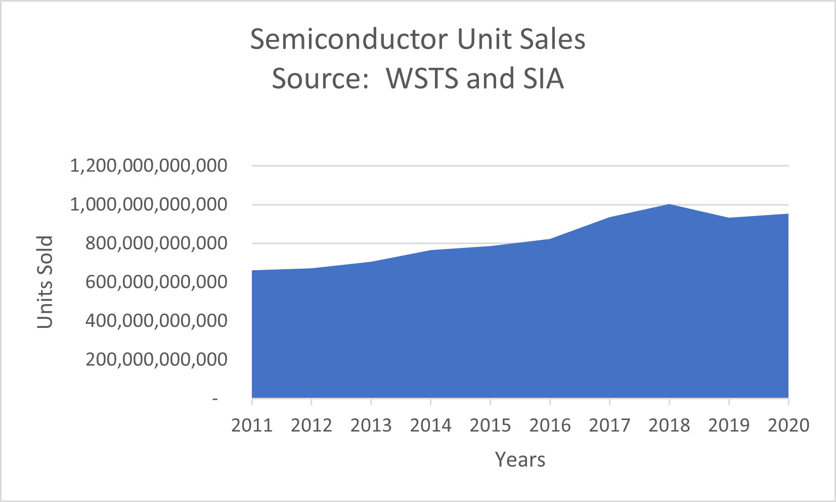
The summation of all of this usage can be seen by the total semiconductor unit volume shipped (Figure Below) from World Semiconductor Trade Statistics Data. Overall, the unit volume of semiconductors has been increasing at a 15+% compounded rate. This is despite the fact that during this time Moore’s law has enabled the doubling of functionality several times over the decade.
So.. what is the “rest of the story” ?
Retail Consumer: Technology shifts such as display technology or system absorption into dominant platforms can indeed cause e-waste tonnage to decline temporarily. However, as these major platforms proliferate more deeply worldwide, the growth of e-waste will likely follow. If another dominant platform becomes viable, the situation may shift even more dramatically.
Non_Retail Consumer: Larger form-factor devices such as appliances, home energy systems (ex..solar), and especially automobiles have an increasing amount of electronics and the resulting e-waste must be handled gracefully.
Centralized Infrastructure: Services such as cloud, transportation control, and communications are all accelerating their use of electronics.
Distributed Infrastructure: With Internet-of-things (IOT) technology, electronics is increasingly embedded in a distributed context in the environment. Because of the large distributed embedded nature, gracefully handling e-waste will become an important factor.
Each of these streams have different characteristics for e-waste collection and disposal.
Overall, electronics usage continues to accelerate and this acceleration adds an enormous amount of value to society. However, the other side of this acceleration is a need to handle the e-waste gracefully.
This is a story of strategic recursion. Yes, a fancy term. I just made up. If you’re not into algorithm development you can Google recursion, but the simple explanation is we’re talking about using the cloud to design the cloud. The story begins with Annapurna Labs, a fabless chip company focused on bringing innovation to cloud infrastructure, now part of Amazon. To more effectively utilize the vast resources of Amazon Web Services (AWS) to build their advanced designs, Annapurna Labs turned to Altair. Altair’s solutions made a substantial impact on these projects and the details of this successful collaboration is the subject of an upcoming webinar. Read on to learn how Annapurna Labs and Altair team up for rapid chip design in the cloud.
First, a little about the presenters. David Pellerin, head of worldwide business development for semiconductor at AWS presents the chip design side of the story. Dave has a long history in EDA, embedded software, chip design and cloud enablement. He is also an author, with several books on FPGA usage and design. Dave has the perfect background to tell the chip design side of this story.
Andrea Casotto
Presenting for Altair is Andrea Casotto, chief scientist, enterprise computing core development there. I’ve known Andrea for a long time. He’s well known to a lot of folks in Silicon Valley. Andrea led Runtime Design Automation for 22 years before being acquired by Altair almost four years ago. Before that he was a researcher at Siemens. Andrea holds a Ph.D. in electrical engineering from UC Berkeley. He has forgotten more about chip design methodology than most people know. He is the perfect person to tell the cloud enablement story. I wrote about a cloud enablement presentation from Andrea here.
Now to the story told during the webinar. There are two key items covered in this event:
An explanation of Altair Accelerator™ Rapid Scaling technology and how it delivers on the promise of efficient chip design on AWS.
A demonstration of how Rapid Scaling works in the Annapurna Labs chip design workflow and a discussion the business merits of this approach
The Annapurna Labs design team was managing workloads on a number of dedicated Amazon Elastic Compute Cloud (EC2) instances and they could occasionally scale up by manually adding new On-Demand instances. However, the process was not automated and led to high touch, forgotten unused compute resources, and either under-scaling or excessive scaling. When you’re dealing with essentially infinite compute resources, inefficiency can get out of hand quickly. The team at Annapurna Labs is designing some very sophisticated technology including AWS Nitro, Inferentia custom machine learning chips, and AWS Graviton2 processors, based on the 64-bit Arm Neoverse architecture purpose-built cloud server. With this kind of complexity, inefficiency can get very expensive.
By deploying a technology from Altair called Rapid Scaling, the efficiency of the design workflow at Annapurna Labs increased by a spectacular margin. You’ll need to attend the webinar to get the exact statistics and how the solution was implemented. A key part of the strategy is something called a license-first approach. The webinar shares details about how Altair’s technology was deployed and what the impact was on the Annapurna Labs design workflow. You’ll be impressed with the results.
The webinar will take place in two time zones, 11:00am CET and 2:00pm EST on April 28. You can choose your preferred time zone and register for the event here. If you’re considering a move to the cloud and are concerned about how to manage costs, I strongly recommend you attend this webinar to see how Annapurna Labs and Altair team up for rapid chip design in the cloud.
There are a lot of articles out right now discussing a possible IPO for Kioxia or sale of the company with Western Digital (WD) and Micron Technology (MT) mentioned as possible acquirers. Kioxia and WD have a partnership for Flash Memory and on March 18th WD gave a presentation on the state of their partnership and what they see as their competitive advantage. With all the recent discussion I though it would be useful to look at Kioxia, how they got to where they are, how the partnership with WD works and what their competitive position is.
Early Flash History
At the 1984 International Electron Devices Meeting, Masuoka, et.al., of Toshiba disclosed the idea of an electrically programable – non-volatile memory that could be rapidly erased in blocks (Flash is for flash erase). The architecture only required a single transistor per memory cell rather than 2 transistors per cell the way standard EEPROM did. This was the beginning of Flash memory technology.
Early Flash memory was weighted towards NOR Flash that was used primarily for code storage. In 1986 Intel invented ETOX Flash and even as late as 2000 Intel was the leading producer of Flash memory with NOR Flash although Intel eventually exited the Flash business before returning to make 3D NAND Flash with Micron.
Around 2005 NAND Flash passed NOR Flash in revenue finding applications in digital cameras, mp3 players, USB memory sticks and other data storage applications. By 2010 NAND Flash represented over 80% of Flash memory revenue and that percentage has continued to grow with increasing use for disk drives and in cell phones.
Up until the mid 2010’s 2D NAND Flash production grew rapidly and led the semiconductor industry with the smallest linewidths, for example 2D NAND was the first application to make use of Self Aligned Quadruple Pattering (SAQP). Eventually 2D NAND Flash cells became so small that a variety of issues drove the need for a new solution, see figure 1.
Figure 1. 2D NAND Scaling Issues.
During this time Toshiba became a leading producer of 2D NAND.
3D NAND
In 2007 at the VLSI Technology Symposium, Toshiba disclosed Bit Cost Scalable Technology (BiCS) for 3D NAND. The BiCS process that was disclosed created a memory stack by depositing alternating layers of silicon oxide and polysilicon and then etching down through the stack to form multiple memory cells in a vertical array. This was a gate first technology and is illustrated in figure 2.
Figure 2. Toshiba BiCS Process.
In 2009 at the VLSI Technology Symposium Samsung disclosed their Vertical Cell Array using TCAT (Terabit Cell Array Transistor) Technology for 3D NAND. TCAT memory array fabrication begins with alternating layers of silicon oxide and silicon nitride and then etching down through the stack to form multiple memory cells in a vertical array. The nitride is eventually removed and replaced with metal layers for the gate and word line (replacement gate).
The TCAT process is illustrated in figure 3.
Figure 3. Samsung TCAT Process.
The basic idea of 3D NAND is to turn the 2D NAND string on end into the vertical direction, see figure 4.
Figure 4. 3D NAND Structure.
The key differences between BiCS and TCAT are:
A BiCS memory array stack is oxide and poly layers and TCAT memory stack is oxide and nitride layers.
In a BICS memory array the poly is left in place and becomes the gates and word lines (gate first). In a TCAT memory array the nitride is removed and replaced with gate metals and tungsten for the gate and word line (replacement gate).
As 3D NAND was being developed there were rumors in the industry that Toshiba could not get BiCS to yield and in fact in around 2014/2015 when the first commercial parts began to filter out, construction analysis done by our strategic partner Tech Insights showed that Toshiba had essentially copied Samsung’s TCAT process. Interestingly Toshiba continued to refer to their process as BiCS even though BiCS and TCAT are fundamentally different processes. I suppose what Toshiba was doing was still “punch and plug” as discussed in the original BiCS paper but in my opinion the process Toshiba took to production is clearly not BiCS.
Kioxia/Western Digital
Due to large losses in their Westinghouse nuclear power division, Toshiba spun out their NAND Flash business into Toshiba Memory and eventually Toshiba Memory was further spun out to an investment consortium led by Bain Capital becoming Kioxia. The approximate ownership shares in Kioxia are Bain at 50%, Toshiba at 40% and Hoya at 10%.
Back when Kioxia was a Toshiba division, Toshiba and SanDisk formed a partnership for Flash memory. Eventually WD bought SanDisk, Toshiba Memory became Kioxia, and Kioxia and WD became partners in Flash memory in a joint venture known as Flash Ventures (FV). FV is owned ~50/50 by WD/Kioxia and the wafer output is split ~50/50.
As I understand the joint venture, Kioxia builds the fabs, Kioxia and WD share the capital expense of equipping the fabs and they share the fabs output with both companies selling Flash memory. In a recent note, Well Fargo noted that the joint venture currently extends to 2034+ presenting a complication to any attempt to acquire Kioxia. The Japanese government also played a role in Kioxia’s formation vetoing too much foreign ownership.
Western Digital Presentation
On March 18, 2021, Dr. Siva Sivaram of WD gave a Flash Technology Overview of the Kioxia/WD partnership. I thought it would be interesting to examine some of the statements that were made in the presentation.
WD and Kioxia have invested a combined $18 billion dollars in Flash R&D in the last ten years, they believe this is the largest investment specific to Flash in the industry. I do not have any data to compare this to.
WD and Kioxia claim >34% of worldwide NAND bits shipped versus 33% for Samsung making the combined entity the world’s largest producer of NAND Flash. I reached out to Bill McClean at IC Insight’s and he provided the NAND revenue breakout shown in figure 5, Samsung has slightly more revenue share than Kioxia/WD. It is entirely possible Kioxia/WD ship slightly more bits and Samsung has slightly higher revenue, overall, I would say that Kioxia/WD is neck and neck with Samsung.
Figure 5. Worldwide NAND Revenue by Company. Figure provided by IC Insight’s.
And interesting note on this, Samsung has revenue of $18.2 billion dollars growing at 21%, Kioxia/WD have combined revenue of $17.6 billion dollars growing at 23% and SK Hynix/Intel has revenue of $11.8 billion dollars growing at 45% (SK Hynix is acquiring the Intel Flash business).
The Yokkaichi fab complex has seen $40 billion dollars in total investment and has over 550 thousand wafers per month capacity (kwpm) making it the second largest capacity fab complex in the world. The reported >550kwpm capacity was somewhat surprising to me, Kioxia has been shedding 2D NAND capacity and a few years ago that number would have made sense to me, but I thought their capacity was closer to 500kwpm in Yokkaichi (Kioxia has another Fab in Kitakami City, Iwate prefecture).
Figure 6 illustrates our estimates for 2D NAND and 3D NAND capacity by company and wafers run.
Figure 6. 2D and 3D NAND Wafer Capacity and Total NAND Wafers Run by Company for 2020.
From figure 6, Kioxia has the highest total NAND capacity but they appear to have more 2D NAND capacity than their competitors and their Fabs are the least utilized. We believe they are shedding 2D NAND capacity currently while also building new 3D NAND capacity. I should note, that getting good visibility on actual 2D versus 3D NAND capacity for Samsung and Kioxia is challenging, and these are best estimate numbers.
During the presentation, several times WD claimed that Kioxia/WD have the best 3D memory cell in the business, I am not sure how they determine this. The physical analysis I have seen from Tech Insights shows identical material sets for the memory cell from Kioxia and Samsung with the only difference being film thicknesses, see figure 7.
Figure 7. Kioxia Versus Samsung Memory Cell.
The thicknesses differences could result in different performance or something about deposition and clean conditions could possibly give Kioxia an advantage in their cell, but it is not clear to me what it actually is or what they are measuring to claim leadership.
WD also claimed multibit leadership and they may have been first for 3 bits per cell – triple level cell (TLC) flash but I believe Intel-Micron was first to 4 bits per cell – quadruple level cell (QLC).
WD claimed that they scale laterally more than the other players and therefore have more bits with fewer layers saving cost. There are multiple elements that go into bit density:
Within the memory array area, bits scale up with number of layers.
Horizontal scaling can increase number of bits per unit area of memory array and could give an advantage in bits per unit area per layer.
Whether CMOS is fabricated next to the memory array or partially under the memory array is a determining factor in what percentage of a die is memory array.
Figure 8. presents an analysis of several generations of 3D Flash parts for layers, bits per millimeter squared, and bit per millimeter squared per layer.
Figure 8. Memory Density.
For each company, Kioxia, Micron (charge trap only), Samsung and SKH there are three columns. The first column is number of layers for the generation, the second column is the bit capacity of the die divided by the die area, the third column is the second column divided by the first column to get bits per millimeter squared per layer.
Black numbers are measured on production parts or conference disclosed numbers, red is our estimates based on layers scaling and forecast for CMOS on the side or under the array. Bold numbers are the leaders for each generation.
Another side note, in their ISSCC 2021 presentation, Kioxia presents 3.88Gb/mm2 for 64L versus our measured density of 3.40Gb/mm2. The ISSCC presentation is for a 512Gb part and the part Tech Insights measured is 256Gb. Similarly, at 96L the ISSCC value is 5.95Gb/mm2 for a 512Gb part and the part Tech Insights measured is once again a 256Gb part. Interestingly the presentation lists a 128L part with 7.8 Gb/mm2 when Kioxia went into production with a 112L part, and they also list 10.45Gb/mm2 for a 170L+ part when their production announcement is 162L. So, there is some disconnect between their presentation and production practices.
Our analysis has SK Hynix leading for bit density and bits per layer at 48 layers, SK Hynix leading for bit density at 64/72 layers but Samsung and Kioxia tied for the bits per layer lead. At 92/96 layers SK Hynix once again leads for both categories. At 112/128 layers we expect Micron to lead for bit density but Kioxia to have the best bits per layers and finally at 160/162/176 layer we expect Micron to lead in both categories. Of course, the Micron values at 112/128 layers and 162/176 are only as good as our forecast and we should note we have not seen any Micron charge trap part analysis yet, so these forecasts are scaled from Micron’s Floating Gate work with Intel. The bottom line is Kioxia appears to be competitive but not be a consistent leader.
The bottom line is who delivers the lowest bit cost, IC Knowledge is the world leader in cost modeling of semiconductor and MEMS. Using our Strategic Cost and Price Model – 2021 – revision 00a we have evaluated wafer cost and bit cost for three generations of 3D NAND by company. Figure 9 presents relative wafer cost, density, and bit cost.
Figure 9. Cost Leadership.
In figure 9 we did not analyze beyond the 112L/128L generation because we are currently updating the model to the latest announced layer counts.
Samsung is the wafer cost leader at all layer counts, this is due to Samsung being the last company to string stack and the last company to put CMOS partially under the memory array. This results in lower wafer cost but eventually the density is not competitive, and Samsung loses out on cost per bit.
The bit cost leadership changes from Samsung at 64L/72L, to SK Hynix at 92L/96L, to Micron at 112L/128L. As mentioned on the figure Micron is the least certain part of the analysis and is subject to change once we see actual measured parts.
In terms of Kioxia, we do not see them the leader in any of the three factors at any layer count analyzed. The Kioxia bit cost is competitive for their 64L process and 112L processes but not at 96L.
In summary we believe Kioxia is a competitive 3D NAND player and particularly strong in bits per millimeter squared per layer, but we would question whether they have the level of leadership represented in the WD presentation.
IPO or Acquisition
This is outside of my specific expertise; it does seem to me that an acquisition by Micron would be difficult with the FV JV in place until 2034+. We estimate WD/SanDisk has invested over $18 billion dollars in equipment located in the Kioxia fabs, how that would be handled in an acquisition and the supply commitments, strikes us as problematic. WD would be the most obvious acquirer, WD did try to acquire Kioxia when they were spun out but lost out to the consortium led by Bain. In a Wells Fargo analysis note they have raised concerns about WD ability to handle an acquisition of the size of Kioxia with a $30 billion price tag mentioned. There may also be issues with the Japanese government blocking the sale of Kioxia to a non-Japanese entity. It seems to me that the most likely outcome is an IPO when the time is right.
Pratik Mahajan, Synopsys VC Formal R&D Group Director, kicked off an absorbing event featuring talks from multiple customers in Europe. He spent some time on formal signoff, an important topic that I’m still not sure is fully understood. Answering the questions “OK, we did a bunch of formal checking but how does that affect total design signoff? And how does this complement dynamic signoff?” A lot of progress has been made here, in areas like formal core coverage, combining formal and dynamic coverage together and accelerating debug through ML-assisted bug triage. Also using formal to accelerate and strengthen low power and safety verification. Lots of meat in this VC Formal SIG.
Keynote on formal today in production verification
Mirella Negra Marcigaglia, Verification Manager at ST Micro Catania, gave the opening keynote on how formal fits into today’s verification challenges. She pushes formal first in development because it’s faster (no TB needed), simpler to use through apps, easier to reuse and of course exhaustive. It’s not perfect: we still need to wrestle with convergence challenges, size constraints, how comprehensive are our properties and whether anything is over-constrained. Mirella makes a very interesting point in her closing slide, that formal skills should be taught much more broadly across design groups. She’s responsible for both, yet in her view formal is easier to pick up than UVM, so should not be limited to a formal-only group. Times are changing.
Modern formal applied to the FDIV bug
In the ‘90s, the Intel FDIV bug catapulted formal from an academic curiosity to a commercial reality. Max Freiburghaus of Imagination Technology shows how this bug would have been caught by modern formal equivalence checking, here in VC Formal DPV (datapath verifier). He goes into detail on the SRT algorithm, showing how approximations inherent in the method can lead to hard-to-reach corner case bugs. And how DPV can find these. You’ll have to concentrate carefully to follow the argument, but worth the effort for a nice demonstration.
When is a bounded proof good enough?
Anthony Wood of GraphCore presented on this topic, which always trips us up. Answering this question isn’t trivial. Perhaps you should increase the proof depth. But that may not be the smart option. Some elements, like counters and memories are between hard and impossible to test exhaustively. And not worth the effort because the great majority of states differ insignificantly from others. You want to cover boundary conditions, unique combinations where bugs may lurk. Anthony talks about a few examples and how formal testbench analysis can help navigate the possibilities. He also throws in a couple of teasers on how formal can help in continuous integration and continuous delivery flows. Nice! Disruptive changes often create new opportunities.
Ultra-low power verification
Another popular topic. Karine Avagian, R&D Formal Verification Engineer and Joakim Urdahl, Sr. Engineer in Verification Methodologies, both at Nordic Semiconductor talked about their work in this area. Joakim has strong background in formal, however adoption in Nordic is relatively recent, so this section covers their first steps to a foundation for ULP checking. Emphasis is on complete property checking, defining properties to describe the complete input/output behavior of a block.
This is an interesting study of first steps into using serious property checking (as opposed to apps). They start with the spec for a block (a UART), define a conceptual state machine for the behavior, then write properties they expect to apply based on that description. Even though this was a learning exercise, they found bugs in the implementation and opportunities for further ultra-low power optimization. For a part that has been in production for quite a while. (Note to self – already in production for years doesn’t mean it’s bug-free.)
Formal versus simulation
Finally, Paul Stravers from the Synopsys Solutions Group presented on eliminating block level sims using formal signoff. This is an eternal quest in formal, their ‘impossible dream’. Which might attract derision, but I like this thinking. We wouldn’t get anywhere interesting without moonshots. Even if/when these projects fail to reach their hoped-for goal, they still make important new discoveries. More power to them. Incidentally, an HSCA is a cluster adapter, commonly used in Ethernet logic. Took me quite a while to figure this out.
You can register to watch the complete VC Formal SIG HERE.
The semiconductor intellectual property (SIP) market is an integral part of the semiconductor industry. Third-party IP has propelled the industry, opening the door for many new products from start-ups to established IDMs. Enabling increasingly complex devices, reducing the cost of product development and reducing the time to market for both leading-edge and mature products are just a few of the benefits of third-party IP.
For the most part, third-party IP has used a business model that employed licensing and royalty fees. This payment arrangement has been successfully adopted by most market players and has matured with the IP market. Over time, we have seen a wide range of licensing and royalty fees depending on the supplier, the volume that is associated with the use of the IP and the complexity inherent to the IP itself. In general, IP users have been constrained by the rules and regulations of closed architectures, even though some of this IP has allowed the market to be highly successful. Over the years, some users of IP have been disgruntled with the lack of design flexibility and the high licensing fees and royalties associated with closed architectures.
Open architecture IP allows users to customize and adapt cores to their own specific applications and provide the opportunity for unique differentiation. RISC-V is an open-architecture Instruction Set Architecture (ISA) that is garnering industrywide attention.
The RISC-V Foundation was established to promote industry adoption and ecosystem collaboration of the RISC-V ISA. In order to gain a better perspective on the current situation, industry perception and future outlook, Semico Research surveyed industry players. Questions revolved around the use and adoption of the RISC-V ISA and its implementation. Semico Research then analyzed the data to develop a forecast for the number of RISC-V cores that will be consumed by the market.
Semico Research conducted a survey (RISC-V Market: Momentum Building) in November 2020 of RISC-V users. This follows an initial survey and report published by Semico in 2019. With this study, we wanted to quantify the total available market (TAM) for IP cores and estimate the served available market (SAM) for RISC-V IP cores. We surveyed and interviewed a cross section of the semiconductor industry to gather information related to the type of devices that are being designed with RISC-V and their target markets.
Semico, in conjunction with the RISC-V Foundation, identified 35 markets and developed both a TAM and a SAM for each of these markets. Utilizing Semico’s extensive end-market databases, we developed a forecast out to 2025. This report focuses on four semiconductor devices which have a high value opportunity to use RISC-V cores. These devices are:
Advanced Performance Multicore SoC
Value Multicore SoC
Basic SoCs, and
FPGAs
Semico’s survey results, RISC-V Market: Momentum Building, indicated increasing interest and significant ongoing developments for RISC-V products in all major end applications. RISC-V devices are also targeted at a broad range of performance levels. The compound annual growth rate for RISC-V cores between 2020 and 2025 is nearly 160%. The fastest growing served available market is automotive which is projected to achieve a 217.7% CAGR.
By 2025, Semico Research predicts that RISC-V cores will capture over 14% of the overall CPU core business. We also expect this trend to continue beyond 2025 as RISC-V gains market share and the ecosystem continues to evolve and mature.
RISC-V’s flexible, open-source strategy provides a competitive advantage which is changing the landscape of the CPU IP market. Other IP vendors have or will expand their architecture to provide an open-source option to maintain a competitive position in the market.
When I started in EDA the big three were Daisy, Mentor and Valid (DMV as we called them). Then came Synopsys in 1986 followed by Cadence, which was a clever merger between ECAD (Dracula DRC) and Solomon Design. Daisy and Valid were pushed aside and then there were, “Three dogs hovering over one bowl of dog food, not a pretty site.” said Joe Costello, former CEO of Cadence, June 1995, CEO Panel discussion, Design Automation Conference.
The fourth comer was Avanti which of course was undone by a “minor” legal problem. I worked for Avanti so I can tell you from personal experience that acquisitions made that company a shooting star and a lazy outside consultant brought it back down to earth. As a result Synopsys acquired Avanti in 2002 then there were three again.
Just a quick note on the Avanti acquisition, Cadence sued Avanti into submission and to save the company from annihilation there was a handshake merger deal with Mentor. Avanti then took that handshake deal to Synopsys and a better deal was made which included extra money for “key” executives meaning the Avanti CEO and his son. Handshake deals meant nothing to Avanti.
Twenty years later the big three EDA dogs are Synopsys, Cadence, and Siemens EDA and the big three have never been bigger. So, how did Mentor become Siemens EDA?
Back in 2011 Mentor attracted the interest of stock activists. In fact, one of the most notorious stock activists, Carl Ichahn, made an unsolicited $1.9B bid saying Mentor must be sold to appease disenfranchised investors. As it turns out Carl was right but his timing was off and so was his price. In 2016 Siemens made a $4.5B offer for Mentor which was accepted but the question is why?
Siemens made the call to Mentor at the right time. The stock was down and activists were again starting to rattle sabers. The real issue was a change in customers: EDA was transitioning from chip companies as the majority of customers to systems companies, and systems companies do business differently.
EDA was really founded on the point tool concept. Point tool companies would bring innovation to EDA with the ultimate goal of being acquired. Chip companies used point tools to get better chips and better pricing from the big EDA companies. Selling just chips is a much smaller margin proposition than systems so EDA budgets were always tight. I remember routinely being told by big chip companies that they were cutting budgets but they wanted more tools.
Systems companies however look for a complete vendor solution covering as many steps in the systems development process as possible. Apple is a perfect example of a systems chip company and now there are many others.
Unfortunately, Mentor had fewer pieces of the systems puzzle than Synopsys and Cadence so they were at a disadvantage. Synopsys and Cadence also had a much more aggressive acquisition strategy than Mentor so the lead was widening.
Now comes Siemens which is the largest engineering solutions company that sells more than $60B to systems companies around the world every year (Synopsys and Cadence combined revenue is around $6B). Definitely a game changer for EDA. And having been with quite a few EDA/IP companies that have been acquired (including by Siemens) I can tell you by experience, Siemens is in this to win this.
So, now we again have three big dogs eating from a larger bowl of dog food, which is much more interesting to watch, absolutely.
Even as Honda Motors puts a so-called Level 3 semi-autonomous vehicle on the road in Japan – 100 of them to be exact – the outrage grows over semi-autonomous vehicle tech requiring driver vigilance. Tesla Motors and General Motors have taken this plunge, creating a driving scenario where drivers – under certain circumstances – can take their hands off the steering wheel as long as they are still paying attention.
Allowing for the hands-off proposition, for some, requires the definition by the system designer of a so-called operational design domain (ODD). This appropriately named protocol describes the acceptable circumstances and functional capability of the semi-automated driving.
The ODD concept is raised in the UNECE ALKS (Automated Lane Keeping System) regulation that defines the enhanced cruise control functionality and the systems and circumstances that make it allowable – including a “driver availability recognition system.” Critics have begun speaking up. The latest is Mobileye CEO, Amnon Shashua.
In a blog post, Shashua asserts that all of these developments represent examples of “failure by design.” By allowing vehicles to drive under particular circumstances, the offending designers are setting the stage for catastrophic Black Swan events because the ODD does not provide for evasive maneuvers, only braking.
It’s worth noting that the main Black Swan scenario envisioned by Shashua is the autonomous driving car following another car, when the leading car swerves to avoid an obstruction and the following autonomous vehicle is incapable of reacting fast enough to avoid the obstruction. Ironically, one of Shashua’s proposed solutions to this problem is to ensure that “the immediate response (of the robotic driver) should handle crash avoidance maneuvers at least at a human level.”
The irony is that in the circumstance of a robotic driver following another car, the robotic driver may in fact be able to respond more rapidly than the human driver. So why should human driving be the standard in all cases? There are clearly circumstances where robotic driving will be superior – too numerous to list here.
Let’s review the UNECE ALKS ODD requirements for semi-autonomous driving – what the Society of Automotive Engineers describes as Level 3 automation:
The Regulation requires that on-board displays used by the driver for activities other than driving when the ALKS is activated shall be automatically suspended as soon as the system issues a transition (from robot driver to human) demand, for instance in advance of the end of an authorized road section. The Regulation also lays down requirements on how the driving task shall be safely handed back from the ALKS to the driver, including the capability for the vehicle to come to a stop in case the driver does not reply appropriately.
The Regulation defines safety requirements for:
Emergency maneuvers, in case of an imminent collision;
Transition demand, when the system asks the driver to take back control;
Minimum risk maneuvers – when the driver does not respond to a transition demand, in all situations the system shall minimize risks to safety of the vehicle occupants and other road users.
“The Regulation includes the obligation for car manufacturers to introduce Driver Availability Recognition Systems. These systems control both the driver’s presence (on the driver’s seats with seat belt fastened) and the driver’s availability to take back control (see details below).”
So the UNECE is very specific about when its ALKS ODD applies. In a recent SmartDrivingCar podcast, hosted by Princeton Faculty Chair of Autonomous Vehicle Engineering Alain Kornhauser, Kornhauser complains that the average driver is unlikely to either study or comprehend the ODD or the related in-vehicle user experience – i.e. settings, displays, interfaces, etc.
For Kornhauser, the inability of the driving public to understand the assisted driving proposition of semi-autonomous vehicle operation renders the entire proposition unwise and dangerous. He also appears to assert that additional sensors are necessary to avoid the kind of crashes that have continued to bedevil Tesla Motors: i.e. Tesla vehicles on Autopilot driving under tractor trailers situated athwart driving lanes, and certain highway crashes with stationary vehicles.
What Shashua and Kornhauser fail to recognize is that Tesla has actually brought to market an entirely new driving experience. While Tesla has clearly identified appropriate driving circumstances for the use of Autopilot, the company has also introduced an entirely new collaborative driving experience.
A driver using Autopilot is indeed expected to remain engaged. If the driver fails to respond to the vehicle’s periodic and frequent requests for acknowledgement, Autopilot will be disengaged. Repeated failures of driver response will render Autopilot unavailable for the remainder of that day.
More significantly, while appropriately equipped Tesla’s are able to recognize traffic lights and, in some cases, can recognize the phase of the signal, when a Tesla approaches a signalized intersection it defaults to slowing down – even if the light is green – and requires the driver to acknowledge the request for assistance. The Tesla will only proceed through the green light after being advised to do so by the human driver.
This operation and engagement occurs once the driver has made the appropriate choices of vehicle settings and may not require that the drive understand the vehicle’s operational design domain. When properly activated, the traffic light recognition system introduces the assistance of a “robot driver” that is humble enough to request assistance.
Regarding Shashua’s concern that a too-narrowly defined ODD, that does not provide for evasive maneuvers, is a failure by design. But appropriately equipped Tesla’s are capable of evasive maneuvers. In fact, appropriately equipped Tesla’s in Autopilot mode are capable of passing other vehicles without human prompting on highways. It’s not clear how well these capabilities are understood by the average Tesla owner/driver.
The problem lies in the messaging of Tesla Motors’ CEO, Elon Musk. Musk has repeatedly claimed – for five years or more – to be on the cusp of fully automated driving. Musk insists all of the vehicles the company is manufacturing today are possessed of all the hardware necessary to enable full self driving – ultimately setting the stage for what he sees as a global fleet of robotaxis.
The sad reality is that these claims of autonomy have displaced a deeper consumer understanding of what Tesla is actually delivering. Tesla is delivering a collaborative driving experience which provides driver assistance in the context of a vigilant and engaged driver. But Musk is SELLING assisted driving as something akin to fully automated driving.
This is where the Tesla story unravels. Current owners that understand and choose not to abuse this proposition view Musk as a visionary, a genius, who has empowered these drivers with a new driving experience.
Competitors of Tesla, regulators, and non-Tesla owning consumers are angry, intrigued, or confused. Some owners may even be outraged at the delta between the promise of Autopilot – as seen and heard in multiple presentations and interviews with Musk – and the reality.
To add insult to injury, those drivers that have suffered catastrophic crashes in their Tesla’s – some of them fatal – have discovered Musk’s willingness and ability to turn on his own customers and blame them and their bad driving behavior for those crashes – some of which appear to be failures of Autopilot. This is the critical issue.
Musk is essentially using his own ODD definition to exempt Tesla of any responsibility for bad choices made by Tesla owners – or even misunderstandings regarding the capability of Autopilot. As a result, Musk’s marketing has indeed given Tesla a license to kill by enabling ambiguous or outright misleading marketing information regarding Autopilot to proliferate and persist.
The collateral impact of this may well be insurance companies that refuse to pay claims based on drivers violating their vehicle’s end user licensing agreement – the fine print no one pays attention to. Musk is muddling the industry’s evolution toward assisted driving even as he is pioneering the proliferation of driver-and-car collaborative driving.
Can Tesla and Musk be stopped? Should they be stopped? How many more people will die in the gap that lies between what Autopilot is intended to do and what drivers think it is capable of? How many is too many?
The saddest part of all is that Musk is an excellent communicator, so there is no question that he knows precisely what he is doing. That somehow seems unforgiveable.
Verification is a resource limited ‘quest’ to find as many bugs as possible before shipping. It’s a long, difficult, costly search, constrained by cost, time and quality. For a multi-billion gate ASIC,
The search space is akin to a space search; practically infinite
In this article we talk about the quest for bugs at the system-level, which it turns out is even more difficult than finding another Earth-like planet humanity can survive on!
FPGA prototyping systems make deep cycles possible for deep RTL bug searches scaled-up to full chip or sub-system level by running real software payloads with realistic I/O stimulus. In fact, with scale-out, you can approximate the throughput of silicon devices.
Terms of reference
Are we on the same page?
Modern FPGA prototyping systems are effective and performant platforms for software development (in advance of available hardware reference boards), system-level validation (demonstrating that the hardware with the target firmware/software delivers the required capabilities), and system-level verification (bug searching/hunting from a system context). Hardware and software bugs can be found in all use-cases. Remember…
Sadly, bugs do remain undetected (even after rigorous searches such as simulation and formal)
Why do hardware bugs escape earlier verification levels such as simulation and formal and what type of bugs can be found when using an FPGA prototyping platform as your verification environment? Hardware and software cannot be developed in isolation. How are you going to ‘validate’ the capabilities of hardware and software combined before committing to silicon? How are you going to validate the ‘target’ system in terms of real software and realistic hardware I/O?
What are the key capabilities that you will need from your FPGA prototyping environment to be successful? Deployed silicon will achieve exacycles (1018) of usage over millions of devices. What are both the achievable and the aspirational targets for ‘deep cycles’ (at least a quadrillion cycles!) of pre-silicon verification, and how do you scale-up to meet these goals?
Hitting the buffers with simulation
You’ve probably met all your coverage goals with simulation. Does this mean all of the bugs have been found? We know you wouldn’t bet your house on it! Consider this for a moment: If you are developing an ASIC or an IP Core that will likely run with a target clock speed in the GHz range; consider how many cycles will run in daily usage and then try to figure out the total number of cycles that you have simulated? You might be surprised (or depressed!).
1e9 and 1e11 cumulative scaled-out simulation cycles is equivalent to only a few seconds of activity
And that’s if you have the servers and licences. You probably have not run the target firmware or software or been able to simulate realistic I/O traffic yet. Are you confident to go to silicon on that basis? Don’t be fooled by great coverage results. As previously mentioned in The Origin of Bugs,
Covered != Verified
How many silicon respins can you afford to address critical design bugs?
If one thinks about actual devices operating at 2-3GHz or greater, and being deployed in the millions, those devices in aggregate are running exacycles (1e18) and greater every day. Now, it’s not the job of verification to simulate the entire lifetime of all devices but,
You need a convincing road-test
Given that, what is the minimum cycle depth we would want to achieve if we want to sleep at night? Companies simply can’t afford to do this with simulation. Emulation goes a long way towards it, but FPGA takes performance and scalability up to another level. The challenge is how to validate designs to this depth, pre-silicon?
The only viable solution is scaled-out FPGA prototyping.
For a modest 1GHz device, consider how many simulation hours are needed to achieve just one hour of target speed equivalent cycles:
Total Simulation time (@100Hz) = 3600x1e9 /100 = 36x1e9 seconds (10M hours)
(or 10K elapsed hours if you can run 1000 simulations in parallel)
The latest FPGA prototyping technologies can achieve speeds from tens of MHz to hundreds of MHz depending on the design parameters. Even here, engineering will need to scale-out the FPGA prototyping capacity to achieve meaningful deep cycle targets.
Approximating to Silicon
As an example, for an FPGA clock speed of say 50MHz, 20 prototype instances will give an equivalent of 1GHz throughput capability. In other words,…
20 prototype instances gets us a piece of silicon to play with!
Scale-out further, and it’s possible to approximate to the throughput of multiple pieces of silicon. So, it’s feasible to achieve deep cycles of pre-silicon verification in a practical timeframe. Of course, the level of scale-out needed depends on achievable FPGA clock speed, the target silicon clock speed, and the depth of testing being targeted.
To find most of the bugs (at least all of the critical ones)
Deep cycles of verification testing alone is not a smart enough goal for our quest.
Hardware acceleration unlocks the ability to run real firmware and software on the RTL
Booting an operating system and then running some software, or rendering a few frames of video, demands long sequences of execution that are not practical with simulation – you can’t wait that long for the test to complete. Emulation takes a big step closer to this capability, and FPGA prototyping takes everything a stage further.
Finding bugs that escape simulation, formal and emulation
Both FPGA prototyping and emulation enable a software-driven approach to system-level verification. Just booting the OS alone is likely to take several billion cycles.
Booting Android takes around 30B cycles; that’s only a few minutes for our 50MHz FPGA, versus several thousand hours for a fast 1KHz simulation! Running the target software or other software payloads such as compliance suites, benchmarks or other test suites, can and does find bugs that will have escaped earlier stages of verification. You might not find a huge volume of such bugs, but when you find them, you know you have…
Saved an escape that otherwise would have made it into silicon
So, the relative value of these bug finds is high. If you then multiply this testing load by the configuration space of both the hardware and the software, you can quickly escalate towards an extremely large volume of testing demand.
When bugs occur, can you detect them?
A really great way to improve failure detection is to leverage SVA assertions from your simulation and formal environments. When SVA’s fire, they pinpoint the failure precisely, which is a huge advantage when you are running huge volumes of testing! You may be able to implement a home-grown flow for adding assertions to your FPGA prototyping environment, or better still, the FPGA prototyping vendor will have already provided a workflow to do this.
Recommendation: Leverage SVA assertions to enhance FPGA-prototyping checking capability
When bugs occur, can you debug them?
Debug consumes a lot of engineering time and this is also the case for an FPGA prototyping approach. There have been many studies[1] of where verification engineers spend their time and most of them show that over 40% of time is spent in debug. Debug is labor intensive, so,
Efficient debug is critical
FPGA prototyping systems necessitate a different approach to debug compared with emulation. You might start the debug process with software debug and trace tools, but from this point onwards you are going to need to debug the hardware, requiring visibility of internal state at the RTL code level. This requires trigger points for events of interest and the ability to extract signal waveforms for debug. It’s an iterative process as the designer zooms-in on the suspicious timeframe and provide enough of the internal hardware state and logic signals to diagnose the bug.
FPGA prototyping systems provide multiple complementary debug strategies to accomplish this. A logic analyzer is required to set up the necessary trigger points to start/stop waveform traces. Debug can be performed at speed, with visibility of a limited subset of chosen signals (probe points), which are then stored to either on-FPGA memory, on-board memory or off-board memory when deeper trace windows are required. This works well, especially when the engineer has a good idea of where to search in the RTL. The limited set of probe points may be more than sufficient to debug most problems.
More complex bugs require full-vision waveform analysis, demanding a different debug approach where full RTL visibility can be reconstructed.
Quest impossible?
No, scale-up and scale-out!
Nothing is impossible, but certain things are hard problems to solve. With many ASIC designs trending to multi-billion gates, prototyping systems need to get bigger, and offer platform architectures that
Scale-up to handle bigger systems and sub-systems
by plugging multiple boards and systems together while minimizing the impact on achievable DUT clock speeds.
You may have started with a lab or desk-based setup, but quickly conclude that you need to deploy an FPGA prototyping cluster (or farm). Deep cycles can be achieved if you
Scale-out to approximate to silicon levels of throughput
Use real-world traffic on a system realistic platform
Advanced FPGA prototyping solutions offer strong build and compile workflows, debug and visibility solutions, and high degrees of flexibility to configure the system to the design needs and cope with devices of any size. Plug-in hardware such as daughter cards allow users to quickly configure the environment to be system-realistic and connect the DUT to real I/O with real traffic profiles. This invariably involves some stepping down of native I/O speeds to the achieved FPGA clock speeds, and it means that the prototyping system needs to be able to handle many asynchronous clocks.
Good automation of the flow (e.g., auto-partitioning) will get you to running your first cycles within a few days. You can then optimize to get the fastest possible throughputs needed to drive towards your approximated-silicon testing goals.
How many cycles to run, is itself, a dilemma; a ‘deep cycles’ dilemma!
In practice this is determined by budget and the capacity available, but the fact is that risk of getting it badly wrong is increasing rapidly. Billion gate designs that integrate a growing array of IP components are required in our modern world to perform ever more complex tasks for applications such as 5G, AI, ML, Genomics, Big Data…the list goes on…
With scaled-out FPGA prototyping you can approximate to the throughput of the final silicon device. But how effective is this software-driven verification approach?
Bug data will be the best metric to measure effectiveness and ultimately the ROI of the investment. Be sure to document and analyze bugs found from FPGA prototyping and assess what the total impact cost would have been had those bugs escaped to be discovered later in costly silicon.
Even if no bugs were found, which is a highly unlikely scenario, there is a value calculation for the assurance that this level of extreme deep testing brings.
Think of it as the “help me sleep at night” verification metric
A true-negative result is just as valuable as a true-positive when it comes to confidence levels and the true value of the final product.
Innovation in technology always creates bigger, better, faster ways of completing the verification quest successfully
Balance the investment between simulation, formal, emulation and FPGA prototyping in a way that reflects the complexity and size of the design, but critically the nature of risk if there were to be escapes. Justifying investment in the quest for bugs is predicated on many factors: the risk of reputational damage and huge rework/mitigation costs can build a strong ROI for investment in FPGA prototyping at scale.
Dan and Mike are joined by Semir Haddad, senior director of product marketing at Eta Compute and Vineet Ganju, vice president and general manager, low power edge AI business at Synaptics. Semir and Vineet discuss the collaboration between Eta Compute and Synaptics to develop new and innovative solutions for AI applications at the edge.
The components of AI systems, both hardware and software are discussed, along with strategies for power reduction. New applications, from building management to farming are also explained.
The views, thoughts, and opinions expressed in these podcasts belong solely to the speaker, and not to the speaker’s employer, organization, committee or any other group or individual.
Semiconductor startups used to rule the roost in Silicon Valley. The very name, Silicon Valley, comes from the birth of the semiconductor industry in the San Francisco bay area 60+ years ago. Large percentage of venture financing used to go to semiconductor startups, even as recently as 15 years ago. As a chip designer doing startups in the late ‘90s and early 2000s in the San Francisco bay area, I felt as if there was a semi startup on every street corner.
Not so much in the last 10 years. Maturing industry, high capital requirements, and dwindling exits have caused a huge decline in funding for semiconductor startups. The narrative of Silicon Valley moved to consumer internet and software-led businesses. Remember, software is eating the world. But in the last few years, we have seen a slow but steady resurgence of semiconductor startups and witnessed blockbuster financing and acquisitions. So, are semiconductor startups on the comeback trail? Or is it a mirage?
First, it is important to separate semiconductor startups from the overall semiconductor industry. Globally, the market for semiconductor products has been growing for several decades and in recent years led by growth in computers, smartphones, consumer electronics, and automotive and industrial electronics. Computers have gotten powerful, phones have faster internet speeds, consumer gadgets have gotten smaller – all because of the technological advances in semiconductors.
Source: “2020 State of the US Semiconductor Industry” from SIA
In a large growing market with improving technology why is there no place for new startups? While semiconductor is maturing as an industry, it is hardly a commoditized market with no place for innovation.
Well, structurally a few things happened:
Cleantech, one of the prominent semiconductor sectors, had flopped badly, losing lots of capital for investors.
The technological advances made in internet infrastructure and mobile technologies led to a boom in the software application ecosystem across social, mobile, and cloud, moving entrepreneurial interest away from semiconductors.
China emerged as a large supplier of semiconductors, thus increasing competition while driving down premiums in the market.
Huge waves of consolidation happened in publicly traded semiconductor companies.
Most sectors go through these phenomena – they are nothing new. When this happens, newer innovations kickstart the next disruption cycle. Why didn’t it happen with semi startups?
Well, the success of a startup ecosystem rests on the number and variety of experiments that are attempted. The more experiments across a wider variety of areas, the better the chances for a breakout success. For semiconductor startups, two main issues slowed down these experiments:
It takes roughly $30M of financing to even get to a product and another $100M or more to get to volume production.
Buyer universe is limited because of the public market consolidation. The reduced list of buyers meant smaller acquisition premiums and smaller exits.
Huge capital costs combined with a small buyer universe and small exits don’t make for an attractive investment area. Combine this with harder macro trend, we saw a vicious cycle of diminishing interest and funding in semiconductor startups.
Things have started turning around over the last few years. Since 2017, investments in semiconductor startups have increased significantly. So, what happened?
One of the main reasons is the explosion of Artificial Intelligence (AI). Innovative semiconductor products were required to meet the computing demand of AI. Advances in AI and Computer Vision helped make huge strides in autonomous vehicles and autonomous platforms. That drove demand for specialized semiconductor sensors and processor architectures.
The cost of building semiconductor products has come down significantly, especially if you are not operating at the cutting edge of semiconductor manufacturing processes. Most semiconductor products do not require these advanced processes. Today, you can build a first-generation semiconductor chip with $10M or less. That is lot less than $30M.
Expanding buyer universe – Apple, Google, Microsoft, Facebook, Amazon, and other large internet and software companies have started building semiconductors for their internal use and consumer products. They have become new acquirers of semiconductor startups.
US-China trade tensions have centered around semiconductors and there has been an increased focus on self-sufficiency and nationalization. This has driven demand for US semiconductor suppliers. Chip shortages facing the automotive industry is driving home the point of self sufficiency.
All these factors have driven huge investments and exits in Semiconductors recently. Just a few examples:
Qualcomm acquired a two-year-old semiconductor startup, Nuvia for $1.4B
Automotive Sensor Semiconductor companies, Luminar, Aeva, Aeye, Ouster and Innoviz all going public at valuation of $1B or more.
Investments flowing into semiconductor startups focused on AI, Quantum computing, Robotics, and others.
So, are semiconductor startups back for good? As new areas come up including Quantum computing, Space technologies, Computational biology … the need for innovation and newer semiconductor products is on the rise. I remain bullish that the resurgence we have seen in semiconductor startups is here to stay. And once again, the name, Silicon Valley, will fit its description.