
The device roadmap for the next few advanced process nodes seems relatively clear. The FinFET topology will subsequently be displaced by a “gate-all-around” device, typically using multiple stacked channels with a metal gate completely surrounding the “nanosheets”. Whereas the fin demonstrates improved gate-to-channel electrostatics due to the gate traversal over the height and thickness of the fin, the stacked nanosheets have further improved this electrostatic control – subthreshold leakage currents are optimized.
An extension to the nanosheet topology that has been proposed is the “forksheet”, as depicted in the figure below. [3]

The goal of the forksheet R&D is to eliminate the nFET-to-pFET device spacing rule (for a common gate input connection), isolating the two sets of nanosheets with a thin oxide. The tradeoff for this attractive gain in transistor density is that the gate again surrounds the channel volume on three sides – “FinFETs turned on their sides” is a common forksheet analogy.
Although the dates for high-volume manufacturing (HVM) of post-FinFET nodes are somewhat fluid, it is expected that these evolutionary nanosheet/forksheet device topologies would emerge in the 2024-25 timeframe.
There is active process development and device research underway for a myriad of alternatives to the nanosheet. Assuming that the “nano” device topology will be used for at least a couple of process nodes, research needs to be aggressively undertaken now, if any new device is to reach HVM in 2028-30.
At the recent IEDM conference, Synopsys presented their forecast and design-technology co-optimization (DTCO) evaluation results for one of the leading device alternatives for the “1nm” node in this timeframe. [1] This article summarizes the highlights of their presentation.
The “1nm” Node
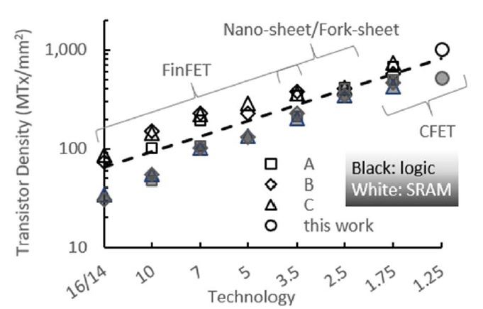
The figure below depicts the straight-line trend of transistor density across several recent process nodes. (This graph was provided as part of collaboration between Synopsys and IC Knowledge, Inc.)

Several things to note about this graph:
- the node names on the X-axis represent a simple transition from the 14nm node, with each successive data point defined by the Moore’s Law linear multiplier of 0.7X
Frequent SemiWiki readers are no doubt aware that the actual nomenclature assigned by a foundry to successive nodes has received some “marketing input”. For the sake of this discussion, using the 0.7X names is appropriate, if the goal of the DTCO process development is indeed to remain on this curve.
- the density data points at each node represent metrics from multiple foundries
- the data points include separate measures for logic and SRAM implementations
Logic density is typically associated with the foundation library cell implementation commonly used with the foundry technology. For example, the area of a 2-input NAND cell reflects 4 devices in the cell using:
- the contacted poly pitch (CPP)
- the number of horizontal metal tracks in the cell (for signals and supplies)
- the cell adjacency isolation spacing (“diffusion breaks” versus tied off dummy gates between cells)
Another key cell dimension is the area of a (scannable) data flip-flop. The transistor density calculation above uses a logic mix of NAND and FF cells for each logic data point.
Of particular note is the assumption for the device topology used in the Synopsys projections for the 1nm node. Active research is underway to evaluate several non-silicon field-effect device types in a timeframe consistent with this node – e.g., 2D semiconducting materials (MoS2) and 1D carbon nanotubes. For the goal of staying on the transistor density curve, the Synopsys TCAD team pursued DTCO process definition for a 3D “Complementary FET” (CFET) implementation. The figure below illustrates the CFET cross-section.

An attractive feature of the CFET technology is the similarity to the nanosheet topology, which will have years of manufacturing experience in the 1nm node timeframe. The novelty of the CFET approach is the vertical positioning of pFET and nFET nanosheets.
The CFET topology leverages the typical CMOS logic application where a common input signal is applied to the gate of both an nFET and pFET device. (The unique case of a 6T SRAM bitcell with nFET-only word line pass-gates will be discussed shortly.)
The figure above illustrates how the pFET nanosheet resides directly below the nFET nanosheet(s). In the figure, two nFET nanosheets are present, narrower than the pFET – as space is required to contact the pFET source and drain nodes, the nFETs are reduced in width. The two nFETs in parallel will provide comparable drive strength to the pFET. (SRAM bitcell design in CFETs utilizes a different strategy.) An M0 contact over active gate (COAG) topology is also shown extending this recent process enhancement.
The processing of CFET devices requires specific attention to the sequential pFET and nFET formation. Epitaxial growth of SiGe for the pFET source/drain nodes is used to introduce compressive strain in the channel for improved hole mobility. pFET gate oxide and metal gate deposition are then performed. The subsequent epitaxial Si growth for nFET source/drain nodes, followed by gate oxide and metal gate deposition, must adhere to materials chemistry constraints imposed by the existing pFET device.
Buried Power Rails
Note the assumption for the 1nm node that the local VDD and GND distribution will be provided by “buried power rails” (BPR), resident below the nanosheets in the substrate. As a result, both “shallow” (device) and “deep” (BPR) vias are required. The metal composition of the BPRs and the vias is thus a critical process optimization to reduce the parasitic contact resistance. The (primary) metal needs to have low resistivity and be deposited with extremely thin barrier and liner materials in the trench.
Speaking of parasitic, the (simplified) layout diagram below highlights a unique advantage of the CFET topology. [2]

The three-dimensional orientation of the CFET devices eliminates the gate traversal between separate nFET and pFET regions. Also, in comparison to a FinFET device layout, the parallel run length of the gate-to-source/drain local metallization is significantly reduced. (The small gate length extension past the nanosheet is shown in the figure.) As a result, the device parasitic Rgate resistance and Cgs/Cgd capacitances are vastly improved with the CFET.
CFET SRAM Design
The implementation of a 6T SRAM bitcell in a CFET process introduces several tradeoffs. The Synopsys DTCO team opted for unique design characteristics, as illustrated below.

- an nFET pulldown : pFET pullup ratio of 2:1 is readily achieved
The two smaller nFET nanosheets shown earlier for a 1:1 logic drive strength ratio are the same width as the pFET in the SRAM bitcell, giving the 2:1 drive strength. (Note that this would be comparable to a FinFET bitcell, where the number of nFET fins is 2 and the number of pFET fins is 1.)
- a modified pair of nFET pass gate devices is implemented
The two nFET nanosheets used for the pass gates are (slightly) weaker than the pull downs; the gate is only present over three sides of the nanosheet. This “tri-gate” configuration provides for a denser bitcell, and optimizes the relative strengths of the pass gate:pull down nFET devices for robust cell read margins.
- the pFET nanosheet under the pass gate devices now becomes an inactive “dummy” gate
- a unique “cross-couple” layer (at the level of the M0 vias) is used for the internal 6T cell interconnections
DTCO analysis early in process development utilizes TCAD simulation tools, to represent materials litho patterning, materials deposition, and (selective) etching profiles. This early optimization work provides insights into the required process windows, as well as the expected materials dimensions and electrical properties, including channel strain to optimize free carrier mobility.
Subsequent parasitic extraction, merged with the device models, enables preliminary power/performance measures for the new process, combined with the device layout area for a full PPA assessment. The (rather busy) figure below provides a visualization of the DTCO analysis for the SRAM bitcell described above.

Summary
At IEDM, the Synopsys TCAD team provided a peek into the characteristics of the “1nm” node, based on a CFET device topology, with one pFET nanosheet below two nFET nanosheets. Buried power rails were also assumed. The lithographic assumptions were based on the utilization of (high numerical aperture) EUV – e.g., a 39nm CPP (with COAG) and a 19nm M0 metal pitch. A unique SRAM bitcell design approach was applied, both for the relative PU:PD:PG drive strengths and for an internal cross-couple interconnect layer.
The results of this DTCO analysis suggest that the 1nm CFET node may indeed be able to maintain an aggressive transistor density, approaching 10**9 transistors/mm**2. It will be extremely interesting to see how this forecast evolves.
I would encourage you to look at this IEDM presentation.
-chipguy
References
[1] Moroz, V., et al, “DTCO Launches Moore’s Law Over the Feature Scaling Wall”, IEDM 2020, paper 41.1.
[2] Ryckaert, J., et al, “The Complementary FET (CFET) for CMOS scaling beyond N3”, VLSI Technology Symposium 2018, p. 141-142.
[3] Collaert, Nadine, “Future Scaling: Where Systems and Technology Meet”, ISSCC 2020, Paper 1.3.
Also Read:
EDA Tool Support for GAA Process Designs
Synopsys Enhances Chips and Systems with New Silicon Lifecycle Management Platform
Synopsys Teams with IBM to Increase AI Compute Performance 1,000X by 2029
Share this post via:


Comments
2 Replies to “What Might the “1nm Node” Look Like?”
You must register or log in to view/post comments.