As a long-time member of the EDA community, I really believe in user groups. EDA tools are complicated beasts, with many options and different ways to use them, and they are constantly evolving. Users interact with their local field applications engineers (FAEs) and sometimes corporate AEs (product specialists) as well on a regular basis. But there is a lot of knowledge on how best to use tools in the R&D teams that develop them. There’s also a great deal of experience spread among the user base, but it’s uncommon for users from different companies to talk directly.
User group meetings are a great way to get a critical mass of users, AEs, and R&D engineers together in one place. It’s best if they’re held in person so that all the participants can interact informally during breaks and meals in addition to the technical sessions. Of course, for now almost every type of meeting and conference is virtual. I was pleased to learn that Agnisys recently held its first-ever user group meeting, which they dubbed AUGER for some mysterious reason. I talked with CEO and founder Anupam Bakshi to find out the scoop.
What is AUGER and what does the acronym mean?
It stands for Agnisys User Group Educational Roundtable, and it is for the most part a traditional user group meeting. It was virtual, as you’d expect right now, but it was a really successful event. There’s also a bit of a pun involved since we wanted to drill down (auger) into technical details and not just present a bunch of fluffy sales/marketing slides.
What were your goals?
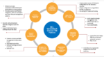
It seems to me that there are three key forms of communication that should occur in a user group meeting: vendor to user, user to vendor, and user to user. The host vendor should present updates on new tools and features, often directly from members of the R&D team, and provide guidance on best practices for using the tools, usually from the field and corporate AEs. The CEO should also offer a company vision and talk about future directions. Second, the vendor wants to hear from the users. It’s really nice to have some user presentations where they share their own experiences and best practices. There should also be a feedback session where the users suggest new tools, features, and support mechanisms to make their lives easier. Last but certainly not least, the users need to interact with each other. That’s harder to accomplish in a virtual format, but we included a roundtable slot where anyone could talk about anything related to Agnisys.
What sort of topics were covered in the technical sessions?
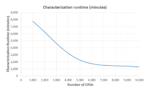
Our engineering team worked hard to develop brand-new slides with the latest and greatest information. Our engineering head summarized the most recent tools and features, many of which were suggested directly by our users. We had a second talk focusing deeply on the latest properties and customizations available for users to tailor our tools to meet their specific needs and fit into their design and verification environments. As you know, we started as a register automation company and this area remains a big part of our business. Accordingly, we held a session dedicated to the quality checks that we do on the register maps provided by users. The more accurate the input maps are, the better the results that we generate for RTL design, UVM testbench verification, embedded C/C++ code, system validation, and documentation. Finally, we had a presentation on how our tools can be used to ensure functional safety and security in chip designs, a hot topic in these days of increasingly autonomous vehicles.
Did the interaction with the users go well?
Honestly, it exceeded my expectations. I have to admit that I was a bit worried about the roundtable, wondering what we would do for 30 minutes if no one spoke up. Fortunately, that was not the case. We had a great facilitator in Tom Anderson, who ensured that we had a lively discussion. We had participation by users from multiple companies, and I was really pleased with that. The attendees were also active participants in the technical sessions, asking lots of good questions. A user from Intrinsix presented an excellent case study on how they benefit from our tools, and other users shared experiences during the roundtable.
Is there anything you might change for future events?
Well, we fervently hope that the pandemic subsides and that we will be able to meet in person next time. We plan on a hybrid event so that users unable or unwilling to travel can still participate. It might make sense to hold multiple events in different regions where we have concentrations of customers. We also hope to add a few more user talks; this first AUGER was developed on a rather tight schedule and not everyone had time to prepare slides. Overall, I expect that we will do many of the same things we did this year because they worked so well.
For those who missed the event, is it possible to access the talks?
Absolutely! We recorded everything, including the roundtable, and it is available on demand. To register, just go to https://www.agnisys.com/events/auger-2021/.
Also read:
Register Automation for a DDR PHY Design
Automatic Generation of SoC Verification Testbench and Tests