In January I presented at the ISS conference a comparison of Intel’s, Samsung’s and TSMC’s leading edge offerings. You can read a write-up of my presentation here.
With the problems going on at Intel, that article generated a lot of interest in the investment community, and I have been holding a lot of calls with analysts who are trying to understand what is going on. Since I presented at ISS and have been participating in calls, I have continued to put effort into analyzing and understanding what is going on with Intel. This afternoon Pat Gelsinger announced Intel’s IDM 2.0 plan to bring the company back to technology leadership.
Before I get to today’s announcements I wanted to start with a little history and how intel got to where they are today.
CEOs
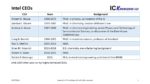
From 1968 until 2005 Intel had four highly technical CEOs, in fact they are among the giants of our industry. The first CEO was Robert N. Noyce, a Ph.D. in physics and a co-inventor of the Integrated Circuit, Next up was Gordan Moore, a Ph.D. in chemistry and the man who coined Moore’s law, the law that has propelled our industry for decades. Moore was followed by Andrew S. Grove, a Ph.D. in chemical engineering. When I first started in the industry, Grove’s book “Physics and Technology of Semiconductor Devices” was the bible of devices and processing, Grove also discovered the Deal-Grove Oxidation law with Bruce Deal. Grove was followed by Craig R. Barrett, a Ph.D. in materials science and professor at Stamford University.
In 2005 Paul S. Otellini, an MBA became Intel’s first non-technical CEO. It was at the end of Otellini’s tenure that Intel began to slip from their process introduction cadence. Otellini was followed by Brian M. Krzanich who has a B.S. in chemistry and a manufacturing background, but, as Stacy Rasgon observed in a recent Podcast, for some reason he never really seemed to get his arms around Intel’s manufacturing issues with substantial yield problems with Intel’s 10nm process on his watch. The podcast is available here.
In 2018 Robert H. Swan, another MBA became CEO and held that position until recently.
I believe a company like Intel that is a historical technology innovator, needs to be led by a technical visionary. Recently Patrick P. Gelsinger has taken over as CEO, he has an M.S. in electrical engineering, was the lead architect for the 80486 and is a well regraded technologist in the industry. Only time will tell but he seems like a good choice to lead a technical turn around.
Figure 1 presents Intel’s CEO history.
Figure 1. Intel CEOs.
Nodes
Figure 2 presents Intel’s nodes versus time and puts into perspective just how dramatic Intel’s delays have been.
In the first column of the table are the node names and in the second column is Intel’s actual introduction dates through 22nm, and then expected dates for subsequent nodes if Intel had kept on the same cadence. From 2001 when Intel introduced 130nm there was a steady two-year cadence of new processes and innovations (the two-year cadence goes back even before 130nm, but I truncated the sequence to make it easier to present). 90nm in 2003 saw the introduction of embedded silicon-germanium for strain, an industry first, 2005 saw the industry’s first use of high-k metal gate (HKMG), something the foundries did not introduce until 28nm in 2011. In 2007 Intel introduced 32nm and finally in 2011, 22nm with the industries first FinFET, something the foundries did not introduce until 2014. Clearly Intel was executing industry leading technologies on a regular cadence.
The third column of the table presents “reset 1” where 14nm was a year delayed to 2014, 10nm was expected in 2017 on a three-year cadence and eventually as 10nm was further delayed 7nm was expected in 2021. The next column has reset 2 where 10nm enters volume production in 2019 and then 7nm is delayed until 2022 originally blamed on COVID. The next column has reset 3 where 7nm production is now expected in 2023, this is an amazing delay for a process that would have been expected in 2017 back when Intel was executing to a two-year cadence. The next column presents “reset 4” based on what could happen if Intel got back on a two-year cadence.
The last two columns present the interval between each process in years and comments on the processes.
Figure 2. Intel Nodes Versus Time.
Hyper Scaling
Intel’s success in introducing industry leading technology in advance of the foundries led to hyper scaling, an acceleration of scaling per node. Historically a typical node delivered 2x the density but now Intel targeted 2.5x for 14nm and 2.7x for 10nm. I believe this played a role in Intel’s slips. If you think about coming up to bat in Baseball, you strike out a lot more when you are trying to hit home runs then when you are trying for singles. Hyper scaling was introduced while the industry was seeing a dramatic increase in process complexity due to multi-patterning.
Figure 3. illustrates Intel’s hyper scaling.
Figure 3. Hyper Scaling.
While Intel has been slipping on process introductions, Samsung and TSMC have been introducing new nodes at a faster rate. The foundries generally take smaller jumps in density but do it more frequently. I believe this reduces risks and increases the rate of learning.
Figure 4. illustrates the foundries introduced five full nodes between 2014 and 2023 while Intel introduced 3 nodes.
Figure 4. Node Introductions.
There are some subtleties this figure does not address, for example Intel has 14, 14+, 14++, 14+++ and 14++++ variants and for 10nm has 10 and now 10SF. However, these plus processes are performance enhancement and do not improve density meaning they are missing out on density improvement learning. The foundries also have “half-nodes not shown here, for example Samsung has 11nm, 8nm, 6nm and 4nm process nodes, and TSMC has 12nm, 7nm plus, 6nm, 5nm plus and 4nm and most of these do provide density improvements.
Culture and brain drain
With Intel’s several year lead on key technologies such as HKMG and FinFETs, Intel had an incentive to not share technical information. Intel was known in the industry to buy tools, bring them in house and not share what they were doing with the Original Equipment Manufacturers (OEM). This helped to protect Intel’s technology but may have also cut them off from taking advantage of the OEM’s increasingly sophisticated in-house process development capabilities. When I first started in the industry, we bought process tools, brought them in house and developed a process to run on them. Today the OEMs provide integrated sets of tools and processes that provide complete process modules.
Internally I have heard that very few people at Intel have a holistic view of a process, that generally engineers only know their tool, if true this would make it difficult to troubleshoot complex interactions between tools.
It is reported that there has also been an exodus of talent from Intel where many of the more experienced engineers have left. I know people who used to work at Intel and told me they had no intension of leaving or retiring but they were offered such generous financial packages that it did not make sense not to leave.
Intel is only as good as their people.
Double edged swords
Intel has two practices that I will refer to as double edged swords because while they provide benefits they also cause problems.
The first one is “copy exact”. At Intel when a process is developed at one of the development fabs, the entire tool set is frozen and when the process is transferred to a production fab an exact replica of the development tool set is installed and set up the same way. This ensures that the process put into manufacturing exactly copies the process that was developed. This helps with initial yield but the downside to copy exact is that as time passes the OEMs are introducing improved tools and even after several years have passed new lines are being set up with tools that are several years old. If you consider Intel was adding 14nm capacity in 2020 and the process was developed around the 2012 timeframe, you can see where this could be a significant issue.
The second issue is nonstandard design flows. Now I am not an expert on design flows, but my understanding is foundries have design flows based on PDKs, with standard cells and relatively simple design rules. I have heard that Intel does a lot of custom tuning of cells. The custom tuning may help squeeze the last little bit of performance out of a design, but it also makes it harder to deal with process changes or port design to a whole new process. Because foundry customers often try to second source parts with more than one foundry, they must be efficient at adapting to different processes. I cannot help but wonder whether this plays a role in Intel’s +, ++, etc. process not including shrinks and also in Intel’s 10nm yield issues.
10nm
Intel’s 10nm process has suffered from well documented delays and yield ramp issues. Intel’s 10nm process was originally targeted to utilize EUV but then due to delays in the development of EUV Intel had to resort to optical multipatterning. It appears that the transition in this process to optical multipatterning did not go smoothly.
For example, at 10nm Metal 0 (M0) and Metal 1 (M1) are patterned with Self Aligned Quadruple Pattering (SAQP) with 2 and 3 cut masks. This is the only use of SAQP in interconnect layers that I am aware of in the industry. Intel’s 10nm M0 and M1 also have the industries only use of cobalt interconnects and aluminum oxide tip to tip spacers I am aware of. The net result is a more complex fabrication scheme for these layers than I believe anyone else in the industry uses. SEM shots I have seen of 10SF M0 and M1 patterns still do not look good compared to foundry 7nm M0 and M1 patterns.
There was a rumor at one point that Intel was going to adopt EUV for a couple of layers for 10SF to address yield issues but that did not materialize, I can’t help but wonder how much the difficulty of porting designs to EUV with the non-standard design flows discussed in the previous section played into that decision.
Node Name Disconnect
There was time when node names for logic processes were the gate length tying them to a specific measurable feature. That is no longer the case and node names today are largely the creation of the marketing departments with no correlation to measurable features. There is a large disconnect between Intel’s node names and the foundry node names. For example, I have taken TSMC’s node names and plotted them versus TSMC’s actual measured transistor density. I have fit a curve to that data and gotten a good curve fit with an R2 value of 0.99, see figure 5.
Figure 5. TSMC Node Names Versus Transistor Density.
Using the formula for the line in figure 5. and actual measured Intel transistor density we can determine equivalent node names for Intel’s processes using TSMC’s trend. The net result is Intel’s 10nm process has a TSMC equivalent node of 7.4nm and Intel’s forthcoming 7nm process is projected to have a TSMC equivalent node of 4.3nm (based on an announced 2x density improvement). Figure 6. presents a comparison of TSMC and Intel processes with TSMC equivalent nodes for Intel processes out to a projected 3nm process. Please note that the values in this table are updated relative to a previous article.
Figure 6. Node Name Disconnect.
From the figure we can see that Intel’s 7nm process falls between TSMC’s 5nm and 3nm process in density. I would like to encourage Intel to consider changing their 7nm process node name to 4nm to more accurately reflect how it compares to TSMC’s industry leading process and address a lot of confusion among analysts on how the processes really compare.
The other interesting observation is if Intel can get back to a two-year node cadence with 2x density improvements around mid-decade they can be roughly at density parity with TSMC although generally about a year behind.
I do want to note that density is not everything, particularly for Intel’s microprocessors where performance is king. As best as I can estimated Intel’s 10SF process and TSMC 7nm process have similar performance, certainly AMD is producing microprocessors on TSMC’s 7nm process that are competitive with Intel’s microprocessors. My expectation is that Intel’s 7nm process will be competitive with TSMC’s 3nm process on a performance basis but with TSMC 3nm entering risk starts later this year and production next year, Intel needs their 7nm process to be complete by the end of next year and ready for high volume production in 2023 or AMD could gain a process advantage by utilizing TSMC 3nm.
In terms of Intel’s catching or passing TSMC, as Stacy Rasgon observed in the PodCast I mentioned earlier, TSMC would have to stumble. I have had several people ask me why Intel does not just accelerate 5nm development. As we will discuss shortly Intel has already struggled with 7nm, a process where the main innovation is EUV that is already in second generation production at Samsung and TSMC. At 5nm I expect Intel to adopt Horizontal Nano Sheets (HNS) a process I believe still has unsolved engineering challenges. Samsung is trying to begin risk starts on their 3nm GAA process using HNS later this year and I am hearing that process is delayed.
IDM 2.0
This brings us to todays presentation on Intel’s IDM 2.0 announcement.
Intel’s key goals are:
- Lead in every product category they participate in.
- Innovate with boldness.
- Execute flawlessly.
- Foster vibrant culture.
As general goals these are great. There appears to be a recognition of the kinds of cultural issues we discussed earlier, and execution definitely needs to improve. A favorite comment of mine from tonight was bringing back a “Groveian culture of execution” in reference to former CEO Andy Grove who was well know for relentlessly driving execution.
The central tenants of IDM 2.0 for Intel are:
- Utilize the Intel internal factory network to build the majority of Intel’s products internally.
- Expand use of foundries so that all products have some level of foundry production.
- Increasing engagement with TSMC, Samsung, GLOBALFOUNDRIES (GF) and UMC.
- Plan to be a major foundry with US and European based manufacturing to balance the reliance on Asia.
There was slide that showed something like 80% of leading edge in Asia centered around Taiwan and South Korea, 15% in the US and 5% in Europe.
The idea of making the majority of product internally while also expanding foundry use is somewhat at odds to each other. It seems like foundry is being used to hedge Intel’s bet on getting 7nm out on time. Also, how do you engage more with foundries while starting a foundry business to compete with them.
There was discussion that Intel is making big investments in industry standard PDKs and simplified design rules. This addresses the earlier comments on Intel’s nonstandard design practices and is both a key enabler for servicing foundry customers and making it easier for Intel to port their own designs to foundries.
There was a lot of emphasis on Intel’s packaging technology with EMIB and Foveros enabling tiles as opposed to chiplets where the quality of the chip-to-chip interconnect is more like long wires on a chip.
Intel is going to partner with IBM on technology, I am not sure I see this as a plus. Samsung and IBM developed the 5nm process Samsung is running and it isn’t competitive with TSMC. They also worked together on the HNS technology in Samsung’s 3nm process and that is even less competitive with TSMC.
Misjudging EUV
I found the comments on the issues with 7nm very interesting. 7nm was developed to limit EUV usage due to “immaturity”. Now that EUV is more mature they have rearchitected and simplified the process using 100% more EUV layers.
What I find particularly interesting is the problems at 10nm can be traced to expecting EUV to be ready before it was and having to redo the process and then at 7nm to underestimating EUV readiness and having to redo the process. This is suggestive of a fundamental problem in Intel’s ability to understand the readiness of a process and appropriately plan for it. This is particularly glaring considering TSMC executing flawlessly on implementing EUV on their 7+ process and 5nm process. Samsung also did a good job of timing EUV with their decision to only have a 7nm process that uses EUV for critical layers (TSMC did an optical 7nm and then EUV 7+ process).
Another area around Intel’s EUV implementation that continues to concern me is availability of tools. I have heard that Intel has pushed out or canceled EUV tool orders during the 7nm delay. If they are pushing out tool to get NXE:3600D tools in place of NXE:3400C tools that makes sense but if they are giving up EUV slots they may not be able to get the EUV tools they need when they need them. TSMC is buying tools to continue to the 5nm ramp, equip for 3nm and for 2nm development, Samsung is doing the same plus has started using EUV for DRAM. SK Hynix recently committed to over $4 billion dollars of EUV tools for DRAM.
Intel has roughly 170k wafer per month (wpm) of 14nm capacity and is ramping 10nm with around 130k wpm of current capacity. If they built out something like 140k wpm of 7nm they could need around 45 EUV tools. They also announced plans for two foundry fabs that could need another 30 EUV tools. Where are they all these EUV tools going to come from?
Foundry pluses and minuses
Part of today’s announcement was that Intel is going to get into the foundry business with a dedicated foundry business with its own P&L and reporting directly to the CEO. Further they plan to build two dedicated foundry fabs in Arizona for approximately $20 billion dollars. I estimate this investment is sufficient for 2 – 40k wpm fabs running 7nm. CORRECTION, these fabs are not dedicated to foundry, they will produce Intel’s own products and also support foundry.
This begs the question of why Intel is doing this and what are the pluses and minuses. The funny part about this is some people have been suggesting Intel should go Fabless and citing AMD going fabless as an example.
Some thoughts on this:
- Pat Gelsinger mentioned that they think foundry is a good business and want to be in it. The interesting thing about foundry is it an excellent business for TSMC but not as good for other leading-edge competitors who have much lower margins. TSMC’s margins for Q4-2020 were around 54%, their next biggest competitor who publicly discloses their results is UMC and their margins for Q4-2020 were only around 24%, SMIC and GF have had many years with negative gross margins.
- Intel was in the foundry business before and failed. Pat admitted they had not been serious about it before. My observation when they were in the foundry business was, they would introduce a new process for their microprocessors and then a year or more would pass before the foundry version was available. To send the message that you are serious in the foundry space, the processes would have to come out at the same time. Pat talked about making the full portfolio of Intel technology available to foundry customers including process technology, IP and packaging technologies. Intel will offer their own cores and support Arm cores.
- Intel plans to build two fabs in Arizona for foundry and then possibly dedicated capacity in Europe in the future, certainly dedicated capacity helps to send the message they are serious and will commit to meet customer needs.
- There is a lot of push right now in the US and Europe for onshore leading edge manufacturing and the promise of subsidy money. Intel could potentially get government money and they are going after department of defense opportunities.
- If you look at TSMC they build a fab for a particular technology and in many cases the fab stays on the technology forever. TSMC is still running 130nm, 90nm, 65nm, 40nm, etc. on 300mm wafers. Somewhat counter intuitively new processes have lower margin because the equipment is depreciating. TSMC often talks about a new process pulling down corporate margins by about two percentage points for the first two years it is in production. Once a fab equipment set is fully depreciated, the wafer manufacturing cost is cut by more than one half but the foundries don’t pass all of the saving on to the customers. The net result is the older fabs generate the highest margins. At Intel all the fabs making processes larger than 32nm have been converted to smaller nodes.
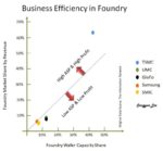
- A key consideration in all this is manufacturing scale. With scale you get more learning, and you can amortize the cost of developing a process over more wafers. This is what doomed GF 7nm, they were only going to build out 15k wpm of 7nm and that was not enough scale to stay competitive. By being in the foundry business Intel can build and maintain more scale. If they do not get in the foundry business, outsourcing to foundries and any market share losses to AMD reduce Intel’s scale potentially starting a death spiral. I was asked on a call whether Intel ran enough wafers to compete with TSMC, TSMC has roughly twice the total 300mm capacity of Intel but Intel’s capacity is concentrated more toward the leading edge meaning they run similar numbers of leading edge wafers, see figure 7.
Figure 7. Critical Mass.
- My big concern in all this is that it will take years to build up this business and engineering talent will have to be diverted to designing, building equipping and starting up the new fabs. Foundry specific versions of processes will have to be developed and PDKs built. This risks taking focus off of what is in my view Intel’s single biggest need right now, and that is to get 7nm out with good yield. Intel is also still struggling to make enough 10nm wafers.
Go Fabless
There has been a lot of talk about why Intel does not just go fabless like AMD did. There are several reasons why this is not a comparable situation:
- AMD went fabless because they had too, they simply could not afford to maintain a competitive fab capability.
- AMD was able to spin out their Fabs with backing from oil money. At the time AMD only had two – 300mm fabs with a combined capacity of around 45k wpm. Intel has roughly 15 logic fabs with around 450k wpm of capacity. Who is going to buy and be able to support that scale of manufacturing? Also keep in mind that GF lost money for a many years, who would be willing to support large losses from the Intel fabs.
- If Intel were to try to transfer all their business to a foundry even TSMC would need many years to build up the capacity. I suppose you could ask TSMC to take over Intel fabs but they would likely want to do a lot of retooling.
- If Intel were to go to TSMC, TSMC’s wafer prices are higher than Intel’s cost and it would drag down Intel’s margins. Intel’s internal manufacturing cost is higher than TSMC’s internal manufacturing cost, but TSMC adds an average gross margin of 54% to their wafers for sale. Although with Intel’s volumes they would pay a significantly lower margin, the margin would still yield wafer prices higher than Intel’s cost. Intel noted this on a previous call discussing this issue.
- In my opinion the best option for Intel is to get 7nm out the door, get back on track and make their products internally. They should hedge their bets at foundries to some extent but if they outsource too much, they lose scale.
To-Do List
I was writing a “What’s Wrong with Intel and How to Fix It” article before today’s call and I had been building my Intel to-do list. Here is my list with where things are after today:
- Hire a technical visionary CEO – Pat Gelsinger must show he can get the job done but he is certainly well regarded.
- Address the culture issues and brain drain – this seems to be recognized as a problem and getting attention. Some key players have returned.
- Adopt industry standard design practices – this was discussed today and is underway.
- Abandon “Copy Exact”, equip fabs with the best tools available at the time and take full advantage of OEMs process capabilities – I have not heard of any discussion on this.
- Go to more frequent new nodes with smaller jumps to accelerate learning and reduce risk – there was discussion today about fixing the development process and getting to a yearly cadence.
- Update node names – align nodes names with what the foundries are doing – I think this would help reduce confusion, but I do not know if it is being considered.
- Get 7nm into production by the end of 2022 and high volume in 2023 – I think this should be Intel’s number one priority.
- This one was not on my list until today, but I think Intel must be careful not to let building a foundry business dilute focus and interfere with execution. This is a lot to take on and frankly I am not convinced this is the right move at this time. Certainly, this could be good for the US, for the electronics industry starved for chips and for the defense department but Intel has to get back on track on process development.
Podcast EP12: A Close Look at Intel with Stacy Rasgon