RVN! 26 Banner revised (800 x 100 px) (600 x 100 px)

Connecting SystemC to SystemVerilog

Connecting SystemC to SystemVerilog
by Bernard Murphy on 09-13-2022 at 6:00 am

UVM Connect

Siemens EDA is clearly on a mission to help verifiers get more out of their tools and methodologies. Recently they published a white paper on UVM polymorphism. Now they have followed with a paper on using UVM Connect, re-introducing how to connect between SystemC and SystemVerilog. I’m often mystified by seemingly overlapping or adjacent efforts between verification capabilities and standards, here in support of co-simulation. My contribution in this article (I hope) is to resolve my own confusion and to answer why this problem is important. I’ll leave the Siemens EDA white paper to handle the details.

Groping through the fog

UVM Connect sounds like it would be a feature of UVM or UVM-SystemC, right? Wrong. UVM Connect is an independent open-source UVM-based library from Siemens EDA, introduced in 2012, enabling TLM communication between UVM/SystemVerilog and SystemC. Conversely, the UVM-SystemC Library 1.0-beta4 was released very recently. However, UVM-SystemC does not support language mixing (as of the current beta release). On the other hand, Siemens EDA is very clear that UVM Connect will continue to be valuable even in the presence of UVM SystemC.

Like I said, confusing. There are areas of apparent overlap, but maybe that overlap isn’t important. UVM Connect is an extension to the UVM standard, invented long before UVM-SystemC, to solve a real problem. Will that solution continue to be relevant? Based on the Siemens-EDA white paper it seems the answer is yes, whatever may happen to UVM-SystemC. Maybe UVM and UVM-SystemC will eventually settle into one standard. In which case I would expect the functionality of UVM Connect to be absorbed in some manner.

Why connect SystemC and SystemVerilog?

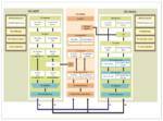
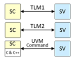
Architectural designers work in SystemC (or C/C++). Implementation designers work in Verilog – SystemVerilog if they are designing testbenches. How do they check/debug the implementation testbench? Ideally by running the architectural model under that testbench. How do they check the implementation model matches the architectural model? Through co-simulation, requiring that they run and compare the SystemC model and the implementation model under the UVM testbench. Both methods can benefit from UVM Connect, connecting the SystemC model to the UVM/SystemVerilog environment and vice-versa.

Equally, having that connection allows verification to use both RTL-based and SystemC-based VIP, expanding and accelerating testbench development. Also some might argue this capability enables UVM to stretch up system level verification. Allowing constrained random tests generated in UVM to be applied to SystemC models. Today, I think that is more of a PSS domain, but the UVM Connect approach certainly works in principle.

Why not use DPI?

Isn’t this getting a little too complicated? SystemVerilog provides a Direct Programing interface (DPI). DPI offers a standard way to connect between SV and C++. Since SystemC is C++, a solution exists; why add another solution? My guess is that the DPI approach is a bit too low level for many of these applications and solutions will invariably be non-portable. In contrast, transaction level modeling (TLM) is a well-established paradigm for handling data exchange between different domains. SystemC is intrinsically TLM-based and UVM provides TLM communication interfaces. UVM Connect simply formalizes this connection in a nice, easy to use way.

My takeaway? UVM Connect is a practical way to connect SystemC models into a UVM testbench in support of implementation verification. Certainly much easier than DPI. More ambitious goals to blend UVM with SystemC and perhaps SystemVerilog may be the long term goal but are not an answer to today’s needs. You can learn more about UVM Connect HERE.


Truechip: Customer Shipment of CXL3 VIP and CXL Switch Model

Truechip: Customer Shipment of CXL3 VIP and CXL Switch Model
by Kalar Rajendiran on 09-12-2022 at 10:00 am

CXL Block Diagram

The tremendous amount of data generated by AI/ML driven applications and other hyperscale computing applications have forced the age old server architecture to change. The new architecture is driven by the resource disaggregation paradigm, wherein memory and storage are decoupled from the host CPU and managed independently through high-speed connectivity. The Compute Express Link (CXL) standard is a direct result of this evolution in the server architecture to support high-speed, low-latency, cache-coherent interconnect. The CXL specification delivers high-performance, while leveraging PCI Express® technology to support rapid adoption. CXL switching features resource pooling, enabling the host CPU to access one or more devices from the resources pool. While CXL 2.0 specification (CXL2) supports single-level switching, CXL 3.0 specification (CXL3) supports multi-level switching wherein the host CPU could leverage different resources in a tiered fashion. CXL3 also introduces fabric capabilities and management, improved memory sharing and pooling, enhanced coherency, and peer-to-peer communication. The spec also doubles the data rate to 64GT/s with no added latency over CXL2.

The specification is also evolving fast, with CXL3 released just three years after CXL1 was released. Truechip has a long track record of offering VIP solutions to a broad list of customers worldwide. It offers an extensive portfolio of VIP solutions to verify IP components interfacing with industry-standard protocols integrated into ASICs, FPGAs and SoCs. As a Verification IP Specialist, Truechip has been offering VIP solutions to support the CXL standard right from the start. For details on their entire portfolio of VIP offerings, visit the products page.  They recently expanded their portfolio with the addition of CXL3 and CXL Switch VIP solutions. You can read their press announcement about first customer shipment of CXL 3 verification IP and CXL switch model.

Truechip’s CXL3 VIP Solution

Truechip’s CXL Verification IP provides an effective and efficient way to verify the components interfacing with CXL connectivity of an IP or SoC. Their CXL VIP is fully compliant with the latest CXL specification. This solution is light weight with an easy plug-and-play interface so that there is no impact on the design cycle time. The solution is offered in native System Verilog (UVM/OVM/VMM) and Verilog.

The following Figure depicts a block diagram of the Truechip’s CXL3 VIP environment.

Some Salient Features

  • Configurable as CXL Host and Device when operating in Flex Bus mode
  • Configurable as PCI Express Root Complex and Device Endpoint when operating in PCIe mode
  • Supports 64.0 GT/s Data Rate with backward compatibility
  • Supports Pipe Specification 6.1.1 with both Low Pin Count and Serdes Architecture
  • Supports Configurable timeout for all three layers
  • Supports different CXL/PCIe Resets
  • Supports Arbitration among the CXL.IO, CXL.cache and CXL.mem packets with interleaving of traffic between different CXL protocols
  • Offers a comprehensive user API for callbacks
  • Provides built-in Coverage analysis
  • Supports all 3 coherency models HDM-D, HDM-H and HDM-DB to access HDM memory

Deliverables

CXL Host/Device

CXL BFM/Agents for:

    • Host and Device sequences
    • Transaction layer (CXL.IO and CXL.cache, CXL.mem)
    • Link layer (CXL.IO and CXL.cache, CXL.mem)
    • Arbiter/Mux layer
    • Phy layer

CXL Monitor and Scoreboard

Test Environment & Test Suite:

    • Basic and Directed Protocol Tests
    • Random Tests Error Scenario Tests
    • Cover Point Tests
    • Compliance Tests

Integration Guide, User Manual, Quick start Guide, FAQs and Release Notes

Truechip’s CXL Switch Model

Truechip’s CXL Verification VIP provides an effective & efficient way to verify the components interfacing with the CXL Switch interface of an IP or SoC. Truechip’s CXL Switch model is fully compliant with the latest CXL specification. The model supports Hot Add and Hot Remove for a CXL Device and is available in native System Verilog (UVM/OVM/VMM) and Verilog.

The following Figure depicts a block diagram of the CXL3 VIP environment when the system implementation incorporates the switching capability.

Aspects Common to All of Truechip’s VIP Solutions

Although covered in an earlier blog, it is worth to reiterate some advantages that cut across all of Truechip’s VIP solutions. All solutions come with an easy plug and-play interface to enable a rapid development cycle. The VIPs are highly configurable by the user to suit the verification environment. They also support a variety of error injection scenarios to help stress test the device under test (DUT). Their comprehensive documentation includes user guides for various scenarios of VIP/DUT integration. Truechip’s VIP solutions work with all industry-leading dynamic and formal verification simulators. The solutions also include Assertions that can be used in formal and dynamic verification as well as with emulations. And, their solutions come with the TruEYE GUI-based tool that makes debugging very easy. This patented debugging tool reduces debugging time by up to 50%.

For more information, refer to Truechip’s website.

Also Read:

Truechip’s Network-on-Chip (NoC) Silicon IP

Truechip’s DisplayPort 2.0 Verification IP (VIP) Solution

Bringing PCIe Gen 6 Devices to Market


WEBINAR: Unlock your Chips’ Full Data Transfer Potential with Interlaken

WEBINAR: Unlock your Chips’ Full Data Transfer Potential with Interlaken
by Daniel Nenni on 09-12-2022 at 6:00 am

Interlaken Blog Post Graphic

Way back in the early 2000s when XAUI was falling short on link flexibility a search for an alternative chip-to-chip data transfer interface with SPI like features lead Cisco Systems and Cortina System to put forward the proposal for the Interlaken standard. The new standard married the best of XAUI’s serialized data and SPI’s flow control capabilities. To this day the continuous growth in data consumption is driving demand for higher speeds, but also lower power-per-bit equating to lower cost-per-bit. Reliability is, of course, also a key requirement. Fortunately, ongoing developments and extensions to the Interlaken Standard allow it to continue to be up to the challenge of current times high bandwidth links. Interlaken has found its way into Applications involving HPC (High Performance Computing), Telecommunications, Data Center NPUs (Networking Processing Units), Traffic Management, Switch Fabrics, TCAMs (Ternary Content Addressable Memories) as well as Serial Memories.

Watch the Replay HERE

Interlaken Operates on packeted data allowing for multiple logical channels to share a common set of High-speed lanes. The data rates on the logical channels can vary which allows for mixing high-speed high throughput data sources with sparsely transmitting occasional usage sources over a shared set of physical lanes. This paired together with rate matching and flow control mechanisms allow for an extremely flexible interface from the perspective of link sharing and data mapping. Data packets can be interleaved such that large packets do not block the link, allowing to balance of the transmission between multiple channels or giving priority to urgent control packets.

Data Integrity and Reliability are achieved with multiple levels of CRC based Error Detection as well as the RS-FEC based Error Correction capabilities. The RS FEC error correction mechanism has been introduced in 2016 as an extension of the standard to address the high BER (bit error rates) of PAM4 links. In case an error occurs, the Retransmit extension from 2010 allows the standard to handle the situation without involving the upper control layers. In this situation the Out of Bound Flow Control interface will be used to request the Transmitter to retransmit data from its internal buffer, to allow for the RX to pick up the data stream at the point the error has been detected and resolve the error.

Other extensions to the interface include the Dual Calendar Extension from 2014, and the Look Aside Extension from 2008. The Dual Calendar allows the addition and removal of channels or change channel priority during operation. Examples of use cases would be for Online Insertion or Removal (OIR) of interfaces or possibly for dynamic re-provisioning of channel bandwidth. The Look Aside Extension defines a lightweight, alternative version of the standard, to facilitate interoperability between a data path device and a look-aside co-processor. It is suitable for short, transaction-related transfers and since it is not directly compatible with Interlaken it should be considered a different operational mode.

Watch the Replay HERE

About Comcores

Comcores is a Key supplier of digital IP Cores and solutions for digital subsystems with a focus on Ethernet Solutions, Wireless Fronthaul and C-RAN, and Chip to Chip Interfaces. Comcores’ mission is to provide best-in-class, state-of-the-art, quality components and solutions to ASIC, FPGA, and System vendors. Thereby drastically reducing their product cost, risk, and time to market. Our long-term background in building communication protocols, ASIC development, wireless networks and digital radio systems has brought a solid foundation for understanding the complex requirements of modern communication tasks. This know-how is used to define and build state-of-the-art, high-quality products used in communication networks.

To learn more about this solution from Comcores, please contact us at sales@comcores.com or visit www.comcores.com

Also Read:

CEO Interview: John Mortensen of Comcores

Bridging Analog and Digital worlds at high speed with the JESD204 serial interface

LIVE Webinar: Bridging Analog and Digital worlds at high speed with the JESD204 serial interface


GM Buyouts: Let’s Get Small!

GM Buyouts: Let’s Get Small!
by Roger C. Lanctot on 09-11-2022 at 6:00 am

GM Buyouts Lets Get Small

“I sell new cars to legitimize my used car business.”  – Wes Lutz, president Extreme Chrysler/Dodge/Jeep, RAM Inc., Jackson, Mich. National Automobile Dealer Association board member

Since taking over at General Motors, CEO Mary Barra has made many radical adjustments in the company’s international footing in the interest of setting the stage for and investing in an electrified future. The company has committed to the creation of multiple large scale Ultium battery manufacturing facilities throughout the U.S. and trumpeted plans for the electrification of the entire GM lineup.

In the process, GM has exited multiple overseas markets including Europe, Russia, Thailand, India, Australia, South Africa, and New Zealand (maintaining some export business in some). Domestically, the company has been rationalizing its North American dealer network.

Two years ago, GM offered buyouts to Cadillac dealers that were unwilling to make six-figure investments in maintenance facility upgrades, charging stations, and employee training in advance of the arrival of the Cadillac Lyriq EV. According to dealer consultant Steve Greenfield, the Cadillac buyouts ranged from $300,000 to $500,000 vs. required investments of $200,000

The Cadillac buyouts reduced the U.S. dealer base by about a third. GM asserted that dealers mainly located in rural areas or non-EV-oriented markets were the focus. (Wouldn’t it be ironic if those bought out Cadillac dealers turned around and added Vinfast or Polestar franchises?)

Now news arrives that Buick dealers are on the chopping block, so to speak, As in the case of Cadillac, GM expects that one third of Buick dealers, like former Cadillac dealers, in rural or non-EV-inclined markets are likely to sever their ties with the brand rather than invest in selling and servicing an EV-only Buick offering expected to take effect in 2024.

The cognitive dissonance of GM’s enthusiastic embrace of EV technology driving an ongoing contraction of GM’s global and domestic vehicle distribution network is extraordinary. Even before these reductions, GM signaled its anticipated departure from sedan segments encompassing such vaunted models as the Malibu, Impala, Cruze, and Regal.

A narrowed lineup of vehicles sold in fewer stores in fewer markets hardly seems to be a recipe for success. The first move was the reduction in the variety of vehicles, which could clearly be seen as a savvy strategy to focus development on a narrower range.

This move made a lot of sense and looks prescient in view of the post-COVID world characterized by troubled supply chains and chip shortages. It also makes sense in the context of a range of EV startups able to focus all of their marketing and sales efforts on one or two vehicles.

The global pullback, too, could be seen as wise. GM was arguably over-extended with limited growth prospects. Subsequent events have borne out the wisdom of these multiple global market departures – especially exits from Russia and Europe, now engulfed in political turmoil and a fuel crisis.

But parting company with one third of an already shrinking dealer base seems uniquely ill-timed. Of course, the key issue is the appearance of GM buying dealers out of their franchises – and for so little! Given the current demand for automobiles generally and EVs, in particular, one might expect dealers to be clinging to their cherished OEM relationships.

In fact, given the importance of EVs to GM’s future one might expect GM to subsidize the needed dealer upgrades. The reduction in Cadillac dealers took the number of locations from 900 down to 565. Buick begins the process with 2,000 dealers.

With Tesla currently boasting approximately 120 service centers in the U.S., a clear picture begins to emerge of a legacy auto maker cutting back distribution (and service) infrastructure while an emerging rival is adding sales and service resources.

GM is on solid ground cutting back on dealers. The conventional wisdom in the industry has long been that there are simply too many new car dealers in the U.S.  Not surprisingly, those numbers have been steadily falling.

Most dealers have seen per-store sales decline, a reversal recently fueled by current vehicle shortages. Yet profits are up along with vehicle prices and markups.

Investors continue to view new car dealers as solid investments with dealer acquisitions on the rise – reflecting an evolving consolidation of distribution. Reducing the number of Buick and Cadillac dealers certainly enhances the value of the dealers that remain in the fold – but a thinning of the dealer ranks will make reaching consumers more problematic.

GM dealers as a group do not make the top ten list of average number of vehicles sold per dealership. Those rankings are dominated today by import makes. Maybe a shorter roster of dealers will improve per-dealer throughput – or maybe it will further erode sales and market share.

It is troubling that GM has determined that it can’t “sell” its own dealers on the prospect of selling EVs. Consumers are lining up to place deposits on new EVs soon-to-be arriving from every make in the market – while hundreds of Cadillac and, soon, Buick dealers are saying: “No thanks.”

In the end, I have to look at GM’s decision from a personal perspective. For nearly every import brand sold in the U.S., I can think of multiple dealer locations that exist within a short distance from my home. When I think of Buick or Cadillac and search for their nearby sales locations, I am looking at a half hour drive or more.

GM’s decisions are clearly financially motivated. The company is marshalling its resources to sell a greatly shortened lineup of vehicles through a diminished network of dealers in a resource constrained market plagued by chip shortages and supply chain snags.

Rather than rallying its retail partners for the coming transformation to new powertrain technology, GM is paying dealers approximately twice as much to quit as it would be asking them to invest to take on the new challenge.

GM is left with a diminished market presence – fewer car models, fewer dealers, fewer overseas markets – and an ever-expanding competitive set of imports and startups. GM literally appears to be self-strangling its way to greater profitability. At the very least a reduction in the size of GM’s dealer network on the eve of massive EV launches sends an ominous message for consumers and investors – and maybe dealers.

Also Read:

MAB: The Future of Radio is Here

GM: Where an Option is Not an Option

C-V2X: Talking Cars: Toil & Trouble


Podcast: Intel’s RISC-V Ecosystem initiative with Junko Yoshida

Podcast: Intel’s RISC-V Ecosystem initiative with Junko Yoshida
by Daniel Nenni on 09-09-2022 at 10:00 am

Welcome to our Podcast on Intel’s RISC-V Ecosystem initiative. I’m Junko Yoshida, Editor in Chief‌ of the Ojo-Yoshida Report. Joining me today to discuss the topic are Vijay Krishnan, general manager of RISC-V Ventures at Intel Corp. and Emerson Hsiao, chief operating officer of Andes Technologies USA

The views, thoughts, and opinions expressed in these podcasts belong solely to the speaker, and not to the speaker’s employer, organization, committee or any other group or individual.


CEO Interview: Jan Peter Berns from Hyperstone

CEO Interview: Jan Peter Berns from Hyperstone
by Daniel Nenni on 09-09-2022 at 6:00 am

DSCF07001

Since 2012, Dr. Jan Peter Berns is the CEO of Hyperstone, a producer of Flash Memory Controllers for Industrially Embedded Storage Solutions. Before that, he held a Senior Manager Position at Toshiba Electronics for several years. Jan Peter brings more than 20 years of management and executive experience in the semiconductor and electronics market.

Hyperstone was founded in 1990 by the German computer pioneer Otto Müller. After selling his previous company “Computertechnik Müller (CTM)” to the Diehl group, he carved together a small team and developed a 32-Bit RISC processor. Starting in 1990, Hyperstone marketed the processor core first as a silicon IP-block later also as a general-purpose microprocessor chip. In 1996 the design was enhanced to become an efficient architectural combination of RISC and DSP making it perfect for the emerging Digital Camera boom. In this context, one of the licensees was Lucky Goldstar, today better known as LG Electronics. LG requested Hyperstone develop a NAND flash controller chip with accompanying firmware. This moment in time was the inception of the company’s product focus today.

What problems are Hyperstone addressing?
NAND flash is inherently unreliable at storing data. Higher densities and complex 3D structures have made data storage exceedingly complex over the last decade. Bit errors, cell wear and tear, deteriorating data retention and read disturbs are just some of the physical effects that need to be mitigated to ensure data can be stored efficiently. Achieving the highest levels of reliability and security, the lowest field failure rates and the best functional safety is Hyperstone’s mission.

What are the solutions proposed by Hyperstone?
Hyperstone is working closely with flash vendors globally to understand the growing complexities of NAND flash failure modes that have come hand in hand with higher density flashes. These insights allow Hyperstone to push the boundaries of reliable NAND flash storage and is one of the many building blocks that enable the company’s controllers to turn NAND flash into storage that lives up to the most critical requirements.

Why should someone choose Hyperstone?
While consumer grade storage is sufficient in cameras, tablets and mobile devices, industrial applications have higher, more intricate demands regarding reliability, availability, and data integrity. This is Hyperstone’s expertise – the insights and experience in designing for industrial grade storage and supporting customers globally throughout the entire design process. From telecom base-band stations to automotive systems to IoT devices and robots operating in the industrial automation setting, Hyperstone has the knowledge to identify the unique demands of any use case and design to its specifications.

Which markets are Hyperstone targeting?
Hyperstone currently serves a range of industrial markets. The strengths of the companies R&D lie in embedded security and reliability, two tenets that gear Hyperstone towards the industrial IoT, security, and automotive markets. The company also supports and has significant experience in industrial automation, telecommunications, the energy sector, medical and transport applications.

What customer problems have you solved thus far?
A lack of use case understanding is the most common and critical issue the company has identified over the years. The assumption that one size fits all, especially for industrial grade applications is the root cause for customers experiencing issues with their storage solutions.

When partnering with Hyperstone on a project, the first question asked is what are the demands of the storage system at hand? By identifying these unique demands, Hyperstone can optimize the flash controller to best support the requirements of the system. At the end of the day, there is no single problem solved; the company optimizes solutions for specific use case demands.

What do the next 12 months have in store for Hyperstone?
Within the next year, Hyperstone will be launching a new SD controller and achieve significant development milestones towards the next eMMC controller. Demand for the company’s products and reliable NAND storage is surging.

Which markets do you feel offer the best opportunities for Hyperstone over the next few years and why?
The companies’ support for all industrial markets worldwide won’t change. Hyperstone does, however, acknowledge the growing demand for reliable and secure storage in the automotive, industrial IoT and security arenas. These are three markets where Hyperstone’s key differentiator’s, reliability and security are crucial.

How is Hyperstone responding to the current semiconductor shortage, especially in the European market?
The current climate of the semiconductor industry has impacted the world. While the company can’t avoid it entirely, Hyperstone has long taken measures to ensure supply shortages are managed as swiftly as possible. This includes buying wafer allocation and tester slots as well as qualifying new substrate and test-service suppliers.

Hyperstone has long established second sourcing for critical process steps to react flexibly to any shortages. To ensure the company’s quality expectations are not compromised, Hyperstone has also accepted increase pricing of major parts. At the end of the day, a strong relationship with suppliers and service providers has ensured the company’s success in these tumultuous times.

And how has the pandemic affected Hyperstone and its customers?
The pandemic impacted Hyperstone’s customer base in unique ways. Different markets experienced different levels of shortages and demands were very volatile as well. While the medical manufacturing market showed significant growth, other markets like the automotive industry were hit hard by the pandemic or supply chain disruptions. Hyperstone was well positioned to benefit from growing markets like medical, 5G and security.

Last question, what is Hyperstone’s future roadmap and direction?
Hyperstone has been growing its R&D teams significantly in the last two years and will continue to do so. The company will expand its portfolio of memory controllers and offer a comprehensive line of storage solutions for industrial and automotive applications. Another major strategic focus is going to be on IoT and security applications.

About Hyperstone
Pioneers in the NAND flash memory controller business, at Hyperstone we design and develop highly reliable, robust controllers for industrial and embedded NAND flash-based storage solutions. We pride ourselves on developing innovative solutions, which enable our customers to produce world-class products for global data storage applications. Our flash memory controller portfolio supports a range of interfaces and form factors including SecureDigital (SD) cards, microSD, USB flash drives, Compact Flash (CF) cards, Serial ATA (SATA) and Parallel ATA (PATA) SSDs, Disk-on-Module (DoM) and Disk-on-Board (DoB) solutions as well as embedded flash solutions such as eMMC.

Also read:

Selecting a flash controller for storage reliability


WEBINAR The Rise of the SmartNIC

WEBINAR The Rise of the SmartNIC
by Don Dingee on 09-08-2022 at 10:00 am

Achronix Webinar - Rise of the SmartNIC

A recent live discussion between experts Scott Schweitzer, Director of SmartNIC Product Planning with Achronix, and Jon Sreekanth, CTO of Accolade Technology, looked at the idea behind the rise of the SmartNIC and ran an “ask us anything” session fielding audience questions about the technology and its use cases.

Three phases of network interface cards

The standards collectively known as Ethernet have made fantastic progress since the early days of “thick net” and vampire tap media attachment units. In those days, simple network interface cards translated packets between the network cable and a parallel bus interface inside a computer, maybe like ISA.

Speeds were not that fast in this first phase of network interface cards, but the simple act of adding Ethernet connectivity opened all kinds of possibilities. The now-famous catchphrase “the network is the computer” defined this era with the ability to move files and send messages easily. Incremental speed improvements continued with successive releases of the standard, a shift to Cat5 cable, more powerful networking chips, and faster bus interfaces up to PCIe.

At higher wire speeds, computers can begin to fall behind even with faster interfaces and chips. Packets can arrive more quickly than some hosts can process them. The second phase, with TCP/IP offload engines, added DMA capability and front-end packet processing like checksums, freeing host processor cycles for other needs. Most flows were raw, with stateless packets, and offload engines mostly offered fixed functions with limited programmability.

For advanced networks, stateful flows are critical to application performance and security. Each flow is set up with its attributes: IP addresses and ports, protocols and applications, user identities, and even content-specific information. Flow tables can be gigantic, with 16M entries or more. In this third phase, a SmartNIC rises to the challenge.

What makes a SmartNIC different?

A few observations about a SmartNICs:

  • Packet processing is soft, fully programmable for any role in today’s network, and able to anticipate future requirements.
  • CPU cores don’t scale well for the high-speed data plane. (The webinar presenters pick on Arm a bit in their discussion, but RISC-V or other CPU cores are at a similar disadvantage. They still play a role in control plane management.) A high-end FPGA can be configured for specific data plane roles and reconfigured on the fly if conditions are detected, such as a denial-of-service attack.
  • Everything needed for stateful flows must run from memory, so FPGA memory performance and interconnect are critical. Technologies like HBM or GDDR6 keep data moving in the FPGA fabric.

Here’s a block diagram of a SmartNIC programmable accelerator based on the Achronix Speedster 7t1500 FPGA, a part combining four 400Gb (or sixteen 100Gb) Ethernet ports with a multi-fractural MAC array and a PCIe Gen 5 interface. Another key in the Speedster 7t architecture is the innovative 2D network on chip, or 2D NoC.  The 2D NoC is a hardened data path which connects all of the FPGA’s external interfaces and memory to each other and deep within the FPGA fabric.  Using the 2D NoC latency is reduced compared to using FPGA logic for data routing across the chip.

Like any workflow-optimized architecture, the theme is to run the Ethernet pipes at speed, keep as many banks of processing and memory as busy as possible, and work on multiple packets in the pipeline. At several points, the presenters mention this is not the high-frequency trading use case, a stateless flow where every nanosecond counts. A few nanoseconds of latency in a stateful flow make little difference at these wire speeds.

Some good questions … and answers

One welcome difference in this Rise of the SmartNIC webinar is that there isn’t much presentation material. After a short preamble with the agenda and some industry factoids, the image above is the only slide in the live stream. More time is spent on audience questions including these:

  • Would a P4 engine run in a SmartNIC?
  • Is “wormhole routing” still a thing, and would a SmartNIC help?
  • Why should both the packet and flow engines be FPGA cores?
  • How does timing closure in the FPGA affect packet processing determinism?
  • What is the role of timestamping in multiple packets from different links?

The answers might surprise you, but you’ll have to watch to find out. This webinar is archived for viewing anytime – follow the link below to register and view the entire discussion.

Achronix Webinar: The Rise of the SmartNIC

Also Read:

A clear VectorPath when AI inference models are uncertain

Time is of the Essence for High-Frequency Traders

How to Cut Costs of Conversational AI by up to 90%


Application-Specific Lithography: 5nm Node Gate Patterning

Application-Specific Lithography: 5nm Node Gate Patterning
by Fred Chen on 09-08-2022 at 6:00 am

Blur Limitations for EUV Exposure

It has recently been revealed that the N5 node from TSMC has a minimum gate pitch of 51 nm [1,2] with a channel length as small as 6 nm [2]. Such a tight channel length entails tight CD control in the patterning process, well under 0.5 nm. What are the possible lithography scenarios?

Blur Limitations for EUV Exposure

A state-of-the-art EUV system has limited options for 51 nm pitch. Assuming the use of sub-resolution assist features (SRAFs) [3], an ideal binary image is projected with good NILS (normalized image log-slope) and depth of focus; however, blur spoils this outcome (Figure 1). The intensity modulation is diminished by blur.

Figure 1. Impact of blur on 51 nm pitch image on a 0.33 NA EUV system. A Gaussian or exponential blur function is convoluted with the blur-free image. Only relative blur magnitudes are given here.

Blur itself cannot be expected to have a fixed magnitude, as secondary electron yield is itself a variable quantity [4]. This alone generates a massive range of possible CDs. Moreover, blur from electrons is more exponential in nature than Gaussian [5]. This further worsens the impact, as exponential blur accumulates more contributions from electrons further away from the point under consideration (Figure 2).

Figure 2. Exponential vs. Gaussian blur. Exponential blur decays faster at shorter distance while Gaussian blur decays faster at larger distances.

Consequently, with CD changes easily approaching or even exceeding 50%, EUV exposure is unsafe for gate patterning, which requires tolerances <10%. High-NA suffers from the same issue. Even if the NA went as high as the vacuum limit of 1.0 (Figure 3), blur, not wavelength/NA, dominates the image.

Figure 3. Blur degrades the ideal image even for the maximum EUV NA of 1.0.

Solution: SADP

The situation is changed entirely if the gate CD is not determined by lithography directly, but by a sidewall spacer width. The lithography pitch for spacer patterning is doubled to 102 nm, which is easily accommodated by ArF immersion lithography. This self-aligned double patterning (SADP) approach has been around for a long time [6,7]. Thus, this gate patterning approach will likely never go away.

References

[1] https://www.angstronomics.com/p/the-truth-of-tsmc-5nm

[2] https://www.dolphin-ic.com/products/standard-cell/tsmc_5ff_cell.html; https://www.dolphin-ic.com/products/standard-cell/tsmc_4ff_cell.html

[3] http://www.lithoguru.com/scientist/litho_tutor/TUTOR43%20(Nov%2003).pdf

[4] H. Fukuda, “Stochasticity in extreme-ultraviolet lithography predicted by principal component analysis of Monte Carlo simulated event distributions in resist films.” J. Appl. Phys. 132, 064905 (2022).

[5] M. Kotera et al., “Extreme Ultraviolet Lithography Simulation by Tracing Photoelectron Trajectories in Resist,” Jpn. J. Appl. Phys. 47, 4944 (2008).

[6] E. Jeong et al., “Double patterning in lithography for 65nm node with oxidation process,” Proc. SPIE 6924, 692424 (2008).

[7] https://seekingalpha.com/article/4513009-applied-materials-smic-move-another-headwind

This article first appeared in LinkedIn Pulse: Application-Specific Lithography: 5nm Node Gate Patterning.

Also Read:


Does SMIC have 7nm and if so, what does it mean

Does SMIC have 7nm and if so, what does it mean
by Scotten Jones on 09-07-2022 at 10:00 am

SMIC 7nm

Recently TechInsights analyzed a Bitcoin Miner chip fabbed at SMIC and declared SMIC has a 7nm process. There has been some debate as to whether the SMIC process is really 7nm and what it means if it is 7nm. I wanted to discuss the case for and against the process being 7nm, and what I think it means.

First off, I want to say I am not going to reveal all the specific pitches, if you want that data you need to purchase a report from TechInsights.

Is it 7nm?

The key pitches for a process technology are Fin Pitch (FP), Contacted Poly Pitch (CPP) and Metal 2 Pitch (M2P). The SMIC pitches for FP are larger than TSMC 10nm FP, and the CPP and M2P are the same as TSMC 10nm. So is this really a relaxed 10nm process, it is not that simple.

The SMIC process also has some Design Technology Co-Optimization (DTCO) features not seen at 10nm. Specifically, TSMC and Samsung 10nm have 8.25 and 8.75 track height respectively at 10nm, SMIC is 6 tracks something that Samsung didn’t do until 5nm and TSMC at 7nm. SMIC also has a Single Diffusion Break (SDB) something Samsung had at 10nm but went away from at 7nm and didn’t get back to until 5nm, and TSMC didn’t implement until their second generation 7nm process (7+).

The bottom line to me is the high-density logic cell density for SMIC is 89 million transistors per millimeter squared, this is very similar to Samsung and TSMC first generation 7nm processes. In my opinion this is a 7nm “class” process and appears to be an acceptable 7nm alternative.

How did SMIC get here

I have seen several comments that SMIC copied TSMC’s first generation 7nm process, and while they may have adopted elements of it, there are a lot of differences too, for example as noted above, all the pitches are relaxed to 10nm or greater dimensions and some of the DTCO features are more advanced than TSMC’s first generation 7nm.

TSMC’s first generation 7nm process was an all-optical process with no EUV layers and due to the US blocking EUV systems from shipping to China, SMIC is limited to an optical approach and this process has no EUV layers.

I find the large CPP dimension particularly interesting. CPP is the combination of gate length, contact width and gate to contact spacer thickness. Gate length is limited by leakage and device type, contact width is limited by a company’s ability to drive down specific contact resistance and therefore achieve an acceptable contact resistance, gate to contact spacer thickness is limited by the capacitance of the spacer material and the resulting gate to contact parasitic capacitance. The fact that the CPP is “10nm like” suggests SMIC is still struggling with these processes. It is common to increase CPP to improve performance and this suggests to me that to get to acceptable performance SMIC had to do that.

Where can SMIC go from here

Assuming EUV systems continue to not be available in China, this limits SMIC’s options for further improvements. It seems likely the US will continue to block EUV shipments to China and I don’t see China developing their own EUV system any time soon.

The most straight forward approach in my view is to reduce the pitches to match TSMC’s first generation 7nm optical process, this combined with the SDB, and 6-track cell would yield a second generation 7nm or even 6nm process. I believe SMIC should be able to achieve this given some time to further optimize the process steps, this could be a reasonable goal for SMIC for 2023. This would contrast with Samsung and TSMC that both have had 5nm in production since 2020 and are currently ramping 3nm, with 2nm in development.

The next obvious question is could SMIC get to 5nm. Without EUV going below 7nm requires increasingly complex multi-patterning with increasingly restrictive design rules and spiraling costs. It is theoretically possible to do 5nm all optical or even 3nm. Self-Aligned Quadruple Patterning with immersion lithography can produce a 20nm pitch small enough for any 3nm requirements but would require a lot of cut masks for Fin and metal patterning to get there.

Conclusion

SMIC appears to have a serviceable first generation 7nm process now with a reasonable prospect to get to second generation 7nm/6nm in the near futures. 5nm and 3nm while theoretically possible would be highly constrained and expensive process versions if pursued due to the lack of EUV.

Also Read:

SEMICON West 2022 and the Imec Roadmap

ASML EUV Update at SPIE

The Lost Opportunity for 450mm

Intel and the EUV Shortage


Samtec is Fueling the AI Revolution

Samtec is Fueling the AI Revolution
by Mike Gianfagna on 09-07-2022 at 6:00 am

Samtec is Fueling the AI Revolution

It’s all around us. The pervasive use of AI is changing our world. From planetary analysis of weather patterns to monitoring your vital statistics to assess health, it seems as though smart everything is everywhere. Much has been written about the profound impact AI is having on our lives and society. Everyone seems to agree that AI software algorithms deliver the transformative technology that powers these changes. Those who are more thoughtful about the process (and perhaps work in the semiconductor industry) realize it is the incredible processing power of semiconductors that brings the software to life. There is a major conference dedicated to hardware and AI coming soon. If you want to learn more, the AI Hardware Summit is the place to be. More on that in a moment. There is another aspect of the AI transformation that is the subject of this post. It is the critical nature of information flow in AI systems. It is here that Samtec is fueling the AI revolution.

Data Everywhere

For a very long time, data was generated by humans interacting with applications. This created something of a self-limiting process. Humans can do so much work per day, so aggregate data grew at a predictable and steady rate. Around 2018 that changed. It was then that machines began generating data. Think autonomous vehicles, aircraft, personal monitoring devices and the ubiquitous use of sensors in almost everything. The fuel for AI is data, so this change had a lot to do with the AI revolution.  A useful measure is a zettabyte, or 1,000,000,000,000,000,000,000 (1021) bytes of information.

According to a Forbes article, there was about .004 zettabytes of data in world in 1997. According to Statista,   the world housed 47 zettabytes of data in 2020. That number is projected to grow to 612 zettabytes by 2030 and 2,142 zettabytes by 2035.  You get the picture.

Applying deep analytics to this data to find the world-changing facts hidden there is a significant benefit of AI. Data is the fuel that powers AI. As processing speed and latency demands grow, more of this processing is being done at the edge or on the device itself. There is simply not enough time to get to the cloud and back. All of this creates substantial complexity in the form of heterogeneous architectures. Many collections of CPU, GPU, DSP, FPGA and custom-built processors working in unison.

All this creates substantial demand on data communication across the architecture. This is where Samtec brings a lot to the table and how Samtec is fueling the AI revolution.

Connectivity Solutions for AI Architectures

Samtec brings value to AI systems design across three primary areas:

  • Next Gen System Expertise: The connectivity solutions provided by Samtec are engineered with the complete system in mind. By taking this big picture approach, all design parameters such as throughput, density, scaling and power/thermal management can be addressed.
  • High-Performance Interconnects: This is the foundational expertise delivered by Samtec. Its large catalog of advanced interconnect solutions offers something for every design challenge. Its ultra-high density, signal-integrity optimized, and high-power interconnects fit well with the challenges of AI system design.
  • Full System Support: Samtec collaborates with its customers. This simple strategy is the margin of victory in many applications. The company’s industry-leading expertise extends the capabilities of any design team, so the entire high-performance signal channel can be optimized.

You can learn more about Samtec on SemiWiki and on Samtec’s website. Here, you can see the full impact of Samtec and its products on high-profile applications, including chipsets, embedded platforms, accelerators, and application-specific architectures.  You will learn a lot.

The Next Big Event

I mentioned the AI Hardware Summit. I attended the first one a few years ago. The conference has grown dramatically since then. It turns out there are many, many AI-focused events. But not that many that focus on the hardware side of AI. This is what brings AI to life and the AI Hardware Summit has a singular focus here.

The event will be September 13-15, 2022 at the Santa Clara Marriott. Samtec will be exhibiting there. You can even get a break on the registration fee if you mention them. See the details below. Stop by and see how Samtec is fueling the AI revolution, live and in person.

Also read:

A Look at the PCIe Standard – the Silent Partner of Innovation

A MasterClass in Signal Path Design with Samtec’s Scott McMorrow

Passion for Innovation – an Interview with Samtec’s Keith Guetig