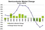
DAC2025 SemiWiki 800x100

CEO Interview: Jaushin Lee of Zentera Systems, Inc.

CEO Interview: Jaushin Lee of Zentera Systems, Inc.
by Daniel Nenni on 07-22-2022 at 6:00 am

Jaushin Lee large

Dr. Jaushin Lee is the founder and CEO of Zentera Systems. He is the visionary architect behind the award-winning Zentera CoIP (Cloud over IP) platform that enables enterprises to dramatically accelerate their journey to Zero Trust security. Jaushin brings 20 years of management and executive experience in networking and computer engineering.

Before Zentera, he was the founder and CEO of Imera Systems, which provided enterprise secure collaboration solutions. He built Imera from the ground up, raised three rounds of funding, and successfully acquired a number of Global 2000 enterprise customers with a multi-million dollar run rate. Earlier, he managed Cisco’s network search engine program, supporting numerous critical product lines, such as the CRS-1 router, Catalyst 4K, and Catalyst 6K, among others.

Jaushin has held management positions with Terawave Communications and Silicon Graphics, as well as an assistant professorship with the EE Department at the University of Virginia. Jaushin earned a PhD from the University of Illinois at Urbana-Champaign, an MS from Columbia University, and a BS from National Taiwan University, all in EE. He has published numerous international conference and journal papers, has been granted a number of U.S. patents, and was recognized as the 2017 CIE Entrepreneur of the Year.

What’s Zentera’s backstory?
I have been involved in many secure collaboration projects during my time at Silicon Graphics, Cisco, and Imera. Many of these projects involved design and technology challenges that required teams from different companies and ecosystems to work together in one environment for optimal productivity.  Each project had unique requirements, we always had to wait for the IT and security teams to provide a customized network environment for each project, which could take months, and sometimes never materialized. I saw some companies create permanent physical chambers for collaboration, but this was only marginally better – developers still had to move their design tools and data into and out of those chambers, which was painful and impacted productivity.  No one seemed to have a solution that was a win-win for everyone!

When I founded Zentera, I set out to fix this problem. We built a virtual chamber that drops around enterprise applications and data to protect them, and incorporated secure access solutions that connect users to their authorized chambers and applications with tight security controls. Everything was software-defined so it could be implemented in minutes, rather than months, and provide a seamless experience for developer collaboration that exceeds corporate security requirements.

Since those early days, we’ve filled out the product offering and refined the security features through deep engagements with EDA powerhouses like Siemens and Cadence, fabless vendors like Ambarella, and manufacturing giants like Delta Electronics. We have built the industry’s most powerful and battle-tested solution for securing sensitive intellectual property.

Recently, the security industry has adopted a lot of the principles we pioneered as part of the Zero Trust security paradigm, and we are seeing application for a wider range of enterprise challenges.  But even today, our CoIP Platform technology is unique in its completeness, especially for protecting enterprise critical intellectual property and applications.

What market segments are you targeting?
Almost all high-tech companies have developed core IP and technology that needs to be protected.  Often, our customers know exactly what they want to protect, but have complex business constraints that often necessitate unpleasant tradeoffs.

You see examples of critical IP throughout the semiconductor value chain: chip design files, verification plans and test vectors, driver source code, or even yield analysis data sets and equipment parameter settings. The complexity of advanced technology designs means that companies can’t do everything in-house; they need a combination of employees, external contractors, and third-party IP or technology vendors to ship on time and on budget. Effectively, this means that third parties in the ecosystem supply chain collaborate on and get access to the crown jewel intellectual property – yet the large corporate network and the fluid nature of projects means most companies don’t have strong controls over who gets access to what.  We solve this problem by helping companies seamlessly contain and control access to intellectual property, regardless of where it’s stored in the company network.

We also work with companies in other market segments outside of high-tech/semiconductors, such as manufacturing, health care, and financial services. While they are each unique, they share a lot of related pain points.

What keeps your customers up at night?
For public companies, cyber security is a common risk item in SEC filings, and not having a good answer for the board if asked whether the corporate IP is secure from cyber attack is a major concern.  Many of our customers have experience with data leak prevention (DLP) solutions, but most of these solutions are “after the fact.”  They may be able to detect data leaving the company, but at that point it’s too late – the data is already gone.  Our customers tell us they selected us because they wanted to block attacks and leaks, not just get a notification or watermark data.

Stealing tech is one level – it’s pervasive enough that the heads of the FBI and MI5 issued a joint statement warning businesses about this.  A next-level fear is that sensitive information, in the wrong hands, could guide a malicious actor to identify attacks to use on devices in the field.  Once shipped, hardware vulnerabilities are nearly impossible to update.

What makes your products unique?
The fundamental challenge for securing intellectual property with traditional network security method is that it relies on discrete boxes in the network.  It’s high touch, very difficult, and expensive to change. CoIP Platform technology is software-defined and doesn’t touch the existing network. It deploys non-disruptively as an overlay to secure IP, whether it’s in a lab, in a datacenter or in the cloud. Whether a customer needs to secure access to data at rest in existing filers, while it’s being processed in the LSF cluster, or as it’s being edited by external contractors, we have solutions to prevent its loss or theft that don’t require IT teams to blow up the engineering datacenter.

What’s next for the company?
The global supply chain concerns of the last few years have highlighted the critical nature of semiconductor manufacturing and its outsized impact on the global economy.  This makes semiconductor manufacturing a target for ransomware groups; and we have already seen some manufacturers being targeted.

Our solutions are powerful not only for protecting EDA tool, semiconductor, and board design, but also for protecting manufacturing and industrial operations, which may include fully-depreciated production lines running outdated operating systems such as Windows XP and Server 2003.  Today our solutions apply to protect smart manufacturing and intelligent industry environments, and we are continuously investing heavily to bring new features to market to make it even easier to adopt Zentera for ransomware protection.

How do customers engage with you? 
Customers who are interested in learning more about how to protect sensitive intellectual property against leaks, theft, and ransomware can contact us through our website (www.zentera.net), or through email (sales@zentera.net) to find a local distributor/reseller.

Also Read:

CEO Interview: Barry Paterson of Agile Analog

CEO Interview: Vaysh Kewada of Salience Labs

CEO Interview: Chuck Gershman of Owl AI


The Silent Revolution is Underway, and Semifore is at its Epicenter

The Silent Revolution is Underway, and Semifore is at its Epicenter
by Mike Gianfagna on 07-21-2022 at 10:00 am

The Silent Revolution is Underway and Semifore is at its Epicenter

There is a major shift in innovation occurring all around us. We see the results every day.  We can interact with them in an easier, more intuitive way. They deliver insights about our health and our daily habits. All this can be categorized as a move towards Smart Everything – ubiquitous machine-assisted intelligence for the good of the planet and its inhabitants. While all this is true, there are some fundamental problems to be solved to get us there. That topic is the focus of this post. Read on to understand how the silent revolution is underway, and Semifore is at its epicenter.

Who is Semifore?

Answering this question requires us to step back a bit in the system engineering process. Today, a “system” is a blend of advanced software algorithms and hardware that implement those algorithms. It is quite clear that software now defines the user experience and those who can deliver the best version of that user experience will win. If you’re looking for an example of how this works, do some research on Apple’s acquisition of PA Semi. This was a key part of a seminal strategy where Apple decided iOS was its lead differentiator, and building a custom processor that would deliver that best experience was the way forward. The company acquired PA Semi, explained the new rules (the software defined the hardware architecture, not the other way) and history was made.

A short time after that decision, Apple surpassed Exxon Mobile as the most valuable company in the world. Today, its lead is unchallenged. So, what is the key technology that drove all this?

There are many. One that stands out is the critical interface between the dedicated hardware that implements the user experience and the software that controls that hardware. This hardware/software interface (HSI) is key to success of any Smart Everything project. The details of how to implement this interface are daunting. The complexity of what’s involved should give every design team pause. How can you get all this right, and not introduce subtle errors that could put future products out of reach?

This is a very real problem. If the HSI contains bugs that are released to the field, those bugs could manifest when a software upgrade is released. Or a new feature, one that is needed for competitive reasons, simply won’t work. The stakes are high. Getting the HSI right is a primary focus of Semifore.

What Semifore Does

When systems were simpler and custom-built processors were rare, the HSI was still complex and important, but easy to keep track of.  Design teams would build spreadsheets to document the control/status registers (CSRs) involved in the process. The values contained in these registers were linked to specific aspects of the hardware’s performance. Once the protocol was specified, it became a matter of tracking the implementation so everyone followed that protocol.

Today, custom-built processors are everywhere, and the complexity of the HSI has exploded. Designs can contain half a million or more CSRs with over a million fields defining various parts of the communication protocol between software stacks and the hardware being controlled. Many of those home-grown spreadsheets have attempted to keep up, but the problem has become too large for do-it-yourself solutions.

The industry has responded to these developments with standards to help define how everything works in a robust and consistent way. While quite useful, each of these standards has its shortcomings. A true, robust executable specification for the HSI is still out of reach in the public standards realm.

Semifore addresses these challenges head-on. Its CSRSpec™ language delivers a robust description of the HSI. Its CSRCompiler™ reads this language, along with the industry standards and creates a correct-by-construction HSI, along with all the formats needed for things like validation, test and documentation. The whole team is in sync with a known-good HSI. This leaves a lot more time to create The Next Big Thing vs. worrying about if it will work.

You can learn more about Semifore on SemiWiki here.

A Customer’s View

Semifore recently published a white paper that details how a large system OEM addressed the challenges of building a robust HSI. The paper goes into detail on the challenges faced, the methodology employed, and the results achieved. I found the piece to be direct, informative, and grounded in reality. If you are struggling with HSI problems, I highly recommend taking a look. You can download a copy of the white paper here.

You will learn that the silent revolution is underway, and Semifore is at its epicenter.

Also read:

Webinar: Semifore Offers Three Perspectives on System Design Challenges

Register Management is the Foundation of Every Chip

CEO Interview: Rich Weber of Semifore, Inc.


EasyVision: A turnkey vision solution with AI built-in

EasyVision: A turnkey vision solution with AI built-in
by Don Dingee on 07-21-2022 at 6:00 am

People counting with EasyVision, a turnkey vision solution from Flex Logix

Artificial intelligence (AI) is reserved for companies with hordes of data scientists, right? There’s plenty of big problems where heavy-duty AI fits. There’s also a space of smaller, well-explored problems where lighter AI can deliver rapid results. Flex Logix is taking that idea a step further, packaging their InferX X1 edge inference accelerator chip in a turnkey vision solution. The best part: it’s pre-trained for specific use cases, so users don’t need any AI expertise to get running.

Lined up for common object detection use cases

We’re not talking about self-driving rocket science. Vision technology is now robust enough to detect sizable objects, like cars through a checkpoint, or people in a room or walkway. Detection accuracy for low-velocity targets in controlled lighting conditions is very high. Scalability is also easy; one or several cameras can interface over Ethernet, USB, or fast Wi-Fi and be brought to one system for processing.

Still, teams who don’t work with AI everyday struggle with implementation. They must find hardware and software, figure out the right AI model for detecting objects, and find or create an AI training data set. Then, they need to put all that together and verify their application works. It can be a very long path to successfully train an application, even for those with AI experience.

What if the training part were already done in a turnkey vision solution? By hand-picking use cases and creating inference software, the EasyVision solution comes ready for a live image feed. Some applications Flex Logix is working on, with a goal of adding two new ones per month:

  • Workplace safety – checking people entering a facility for visible gear such as hardhats can be automated.
  • People counting – retailers, schools, and event centers can count how many people enter a building, occupy a specific room, or pass through an area.
  • Health monitoring – face mask compliance checks are easy with vision detection.
  • Vehicle access – how many cars, how many open spaces, and how long each car has been inside a parking facility are also easy detection tasks.

YOLO-based recognition at up to 60fps in less than 10W

Running AI inference efficiently is also a big piece of the equation. Quite a few convolutional neural network (CNN) algorithms can do object detection. YOLO (in this case, You Only Look Once) is a one-stage detector algorithm which finds regions and classifies objects in one pass. The result is excellent real-time object detection performance. YOLO continues evolving, with recent versions improving frame rate without compromising accuracy.

YOLO also maps cleanly to the InferX X1 chip, designed for efficient low-power AI inference – not video gaming. Its tensor processor units, or TPUs, are tiled and reconfigurable dynamically for many CNN models. In an AI development workflow, a customer would use the InferX DK tool chain to compile their preferred trained model into the InferX X1. In the EasyVision solution, Flex Logix has already done that work for the YOLO algorithm and object training data sets.

The EasyVision solution runs object detection at up to 60fps HD images from multiple cameras in real-time, using less than 10W of power. The InferX X1 chip is comes on either a PCIe or M.2 card, allowing installation in many hosts – including Dell and HPE platforms. Users get software to install pre-trained object detection models of choice. There’s also a software API for integrating detection results into a high-level application.

As the portfolio of EasyVision-trained applications expands, more users will see the power of a turnkey vision solution. EasyVision gets a vision-enabled object detection application off the ground with no AI learning curve. Teams looking to launch a broader AI initiative may want to start with an EasyVision package to pilot a concept. Then, they can step up to creating models and configuring the InferX X1 chip, leveraging its low-cost, efficient AI inference.

For more info, please visit the Flex Logix EasyVision webpage.


DSPs in Radar Imaging. The Other Compute Platform

DSPs in Radar Imaging. The Other Compute Platform
by Bernard Murphy on 07-20-2022 at 6:00 am

Radar Trends

In the flood of CPU and GPU announcements in pursuit of new technology advances, it is easy to lose track of another kind of platform – DSPs. Digital signal processors, once a niche platform for specialized applications, are now front and center in some of the hottest technologies. Because their strength in signal processing has become key to making those technologies work. Radar imaging is one good example.

4D imaging

In automotive applications we all know about visual imaging and object detection. Cool stuff but it suffers from a couple of important drawbacks. First, it only works well in good seeing conditions, not so well at night or in bad weather. Second, it is primarily 2-dimensional and has no sense of relative velocity or even of distance. It detects an object but is that object near or far away? Is it stationary or moving towards you rapidly?

LIDAR gets a lot of press as a complementary 4D detection method (3 spatial dimensions plus velocity). This can work in bad weather and does provide relative velocity. Radar, also able to sense velocity, was still seen as a useful but coarse technique. Good enough for “something is approaching rapidly from the front or the back of the car, but that was about it.

Radar steps up to imaging

But then radar designers got ambitious with their own 4D option, now able to sense distance and direction in a 2D plane, relative velocity and also vertical information (will I fit under that overpass?) The design starts with an array of up to 200 antennae which can transmit and receive radar signals.  These are still wide beams, now combined through a technique known as beamforming to separate distinct reflections with high accuracy (<1o). This is the same MIMO technique used in 5G.

After noise filtering and corrections, this data is aggregated into a 4D point cloud, similar to the LIDAR approach and object detection, sensor fusion and other operations can run on that data. Following the trend to smart sensing, radar imaging now does most of this analysis at the sensor to avoid latencies and communication overhead in the car network. This sensing is central to safety, so the computation must be fast yet it also must be economical on power.

DSPs – the right solution to radar imaging

Start with beamforming. This is an ultimate signal processing application – teasing a fine resolution signal out of multiple broad resolution reflections. It requires floating or fixed-point analysis because you’re dealing with analog signals after all. Complex signals, if the radar uses complex modulation. And massive parallelism, processing input from ~200 antennae. This task is far beyond the capabilities of CPUs and GPUs but plays directly to the strengths of DSPs.

Other platforms can handle building the point cloud and inferencing . But if you’re already in a DSP that can also handle these functions very well, why switch? Adding more components increases the bill of materials and cost, increases latencies and power and challenges reliability. DSPs are already widely used in machine learning applications with well-established interfaces to all the common ML networks.

Which suggests that platforms like the Tensilica ConnX 110 and 120 IP need a closer look. These compact low-energy platforms improve upon the already popular BBE32EP and BBE16EP platforms, adding to a proven product line for radar, lidar and communications. With a track record in radar imaging with companies like NXP and with differentiated strengths in processing complex data, Tensilica looks like a strong contender in this space.

You can learn more about the ConnX product family HERE, HERE and HERE.


OpenFive Joins Universal Chiplet Interconnect Express (UCIe) Consortium

OpenFive Joins Universal Chiplet Interconnect Express (UCIe) Consortium
by Kalar Rajendiran on 07-19-2022 at 10:00 am

Snapshot of Contributing Members of UCIe

Universal Chiplet Interconnect Express (UCIe) is an open specification that defines the interconnect between chiplets within a package. The objective is to enable an open chiplet ecosystem. Although the initial specification for UCIe was developed by Intel, a consortium was announced in March with Intel, AMD, Arm, Google, Meta, Microsoft, ASE Group, Qualcomm, Samsung and TSMC as its promoting members. The promoting members represent a diverse functional cross section of semiconductor ecosystem expertise. Just in the three months since the consortium’s formation, many companies have joined as contributing level members (see Figure below).

That is a lot of committed members keen on progressing this universal interface standard. Each of these members brings its unique expertise to the consortium and of course expect their involvement to further their own business goals as well as the industry’s progress. OpenFive announced their membership recently and this post will look at what that means for them as well as for the consortium and the industry. The post will review OpenFive’s history and track record, its UCIe membership, and its pending acquisition by Alphawave. In essence, its Past, Present and Future.

Past

The OpenFive team has been delivering custom silicon for over 15 years. The key to increased productivity is leveraging pre-verified IP subsystems and OpenFive has built many such IP subsystems to support its customer base. These IP subsystems address connectivity and memory interfaces. You can learn more at their IP portfolio page.

As chiplets-based development started picking momentum a few years ago, OpenFive started playing an instrumental role to support this movement. OpenFive developed a die-to-die (D2D) IP subsystem. The subsystem supports low-power, high-throughput, and low-latency links enabling quicker integration for heterogenous chipset connections in wired communications, AI and HPC applications. It introduced the industry’s first Die-to-Die (D2D) Controllers which are agnostic to physical link interfaces, thereby supporting OHBI and BoW interfaces for chiplets. You can learn more from a SemiWiki post published last year.

Present

The current industry trend for scalable silicon architectures makes efficient and standardized Die-to-Die and Chip-to-Chip interconnects critical for SoC solutions. This has created a need for strong experience in advanced packaging, test, and production in leading-edge process nodes such as 5nm as well as older nodes. OpenFive is staying ahead by investing in die-to-die (D2D) interfaces, chiplet technology and 2.5D packaging. They can support chiplets that enable partitioning of the design into different functions, and the option to choose a process optimized for that particular function.

With their capabilities to engage in a spec-handoff, netlist handoff or production handoff, OpenFive can service their customers, whether a chiplet interface standard exists or not. But a standard such as the UCIe interface certainly makes it easier, faster and consistent and is expected to accelerate the growth of chiplet based products market.

The addition of support for UCIe support is a natural progression to their existing support for OHBI and BoW interfaces. As a contributing level member of the UCIe consortium, OpenFive will actively participate in the Electrical and Protocol subgroups. They get to drive the specification and influence the direction of the technology. And, of course access the intermediate (dot level) specifications. OpenFive will leverage its depth of experience from multiple customer engagements and its silicon platforms.

Future

In March of 2022, Alphawave IP Group announced a definitive agreement to acquire OpenFive. The transaction is expected to close in the second half of 2022. As per that press announcement, the acquisition will enhance Alphawave’s chiplet design capabilities. The combined company will offer an expanded die-to-die connectivity portfolio that will accelerate chiplet delivery capabilities to customers. The acquisition will nearly double the number of connectivity-focused IPs available to customers. Post-acquisition, the company will become a one-stop-shop for customers bundled connectivity needs in the most advanced technologies at 5nm, 4nm, 3nm and beyond.

Customers looking to implement their chiplet-based SoCs for Cloud/Datacenter, AI/HPC, and Networking applications can expect to benefit by leveraging OpenFive’s leading-edge custom silicon implementation and advanced 2.5D packaging capabilities together with their highly optimized memory and connectivity IP subsystems.

Also read:

IP Subsystems and Chiplets for Edge and AI Accelerators

A 2021 Summary of OpenFive

Enhancing RISC-V Vector Extensions to Accelerate Performance on ML Workloads


Future Semiconductor Technology Innovations

Future Semiconductor Technology Innovations
by Tom Dillinger on 07-19-2022 at 6:00 am

2D metals

At the recent VLSI Symposium on Technology and Circuits, Dr. Y.J. Mii, Senior Vice President of Research and Development at TSMC, gave a plenary talk entitled, “Semiconductor Innovations, from Device to System”.  The presentation offered insights into TSMC’s future R&D initiatives, beyond the current roadmap.  The associated challenges of the technologies being investigated were also highlighted.  This article summarizes Dr. Mii’s compelling presentation.

Technology Drivers

Dr. Mii began with a forecast for future end market growth, emphasizing both the need for continued gains in high-performance compute throughput and the focus on power efficiency.  For the HPC requirements, he shared a “digital data boom” forecast, shown in the figure below.  For example, a “smart” factory will be expected to collect, monitor, and analyze 1 petabyte of data per day.

The role of machine learning (training and inference) support for the applications above is likewise anticipated to expand as well, putting further demands on the HPC throughput requirements.  Dr. Mii commented that these HPC requirements will continue to drive R&D efforts to increase logic density, both in the semiconductor process roadmap and advanced (heterogeneous) packaging technology.

The relentless focus on power efficiency is exemplified by the slide below.

The architecture shown illustrates not only the extent to which 5G (and soon, 6G) will be pervasive in the devices we use, but also in the operation of “edge data centers”.  As with HPC applications, the influence of machine learning algorithms will be pervasive, and needs to be focused on power efficiency.

Recent Technology Innovations

Before describing some of TSMC’s R&D projects, Dr. Mii provided a brief summary of recent semiconductor process technology innovations.

  • EUV lithography introduction at node N7+
  • SiGe pFET channel for improved carrier mobility
  • Design Technology Co-optimization (DTCO)

Dr. Mii emphasized how process technology development has evolved to incorporate much greater emphasis on DTCO, that evaluating tradeoffs between process complexity and design improvements has become an integral part of process development.  He highlighted recent adoption of contact-over-active-gate and single diffusion break process steps as examples.  He added, “DTCO efforts are not exclusive to logic design – memories and analog circuitry are a key facet to DTCO assessments, as well.”

  • nanosheets (at node N2)

TSMC will be transitioning from FinFET devices to a nanosheet device topology at the N2 process node.

Future Semiconductor Technology Innovations

Dr. Mii then described several semiconductor technology R&D efforts for future application requirements.

  • CFET (complementary FET)

After decades of planar FET device technologies, FinFETs have experienced a considerable longevity as well, from N16/N12 to N7/N6 to N5/N4 to N3/N3E.  It will be interesting to see how process nodes based on nanosheet devices evolve.  After nanosheets, Dr. Mii focused on the introduction of CFET devices.

As illustrated in the figure below, a CFET process retains the benefits of the gate-all-around nanosheets, yet fabricates the pFET and nFET devices vertically.  (In the figure, the pFET is on the bottom, and the nFET is on the top.)

In the cross-section of the inverter logic gate depicted above, the common gate input and common drain nodes of the two devices are highlighted.

The figure below expands upon the process development challenges introduced by the CFET device stacking, especially the need for high aspect ratio etching and related metal trench fill for the vertical connectivity highlighted above.

NB:   Different researchers investigating CFET process development have been pursuing two paths:  a “sequential” process where pFET and nFET devices are realized using a upper thinned substrate for top device fabrication that is bonded to the starting substrate after bottom device fabrication, with an intervening dielectric layer;  a “monolithic” process where there is a single set of epitaxial layers used for all devices on the substrate.  There are tradeoffs in process complexity and thermal budgets, device performance optimizations (with multiple substrate materials in the sequential flow), and cost between the two approaches.  Although Dr. Mii did not state specifically, the comments about high AR etching and metal fill would suggest that TSMC R&D is focused on the monolithic CFET process technology.

  • 2D Transistor Materials

There is active research evaluating “post-silicon” materials for the field-effect transistor channel.  As shown below, as the device gate length and body thickness of the channel are reduced, 2D materials offer the potential for both improved carrier mobility and sub-threshold slope (with lower leakage currents and the potential for lower VDD operation).

One of the major challenges to 2D process development is to provide low contact resistance connections to the device source/drain nodes.  Dr. Mii shared results previously published by TSMC researchers highlighting the evaluation of bismuth (Bi) and antimony (Sb) – a 5X reduction in Rc over previously published work was achieved, as shown below.

  • BEOL interconnect architecture

Scaling of the back-end-of-line interconnect is encountering the challenge that existing (damascene) Cu wires are less effective.  The Cu diffusion barrier (e.g., TaN) and adhesion liner (e.g., Ta) in the damascene trench occupies an increasing percentage of the scaled wire cross-section.  The Cu deposition grain size is constrained as well, resulting in greater electron scattering and higher resistivity.  The figure below highlights TSMC R&D efforts to introduce a new (subtractive-etched) BEOL metallurgy.

With a subtractive metal process, new opportunities for fabrication of the dielectric between wires are introduced – the figure above illustrates an “air gap” cross-section within the adjacent dielectric.

  • 2D conductors

Beyond a replacement for Cu as the BEOL interconnect described above, TSMC R&D is investigating the potential for 2D conductors.

The figure above shows a cross-section of 2D conductor layers, and the resulting conductivity benefits compared to a comparable Cu wire thickness.

(Dr. Mii did not elaborate on the specific materials being evaluated.  For example, there are a number of transition metal compounds that demonstrate high carrier mobility in a 2D crystalline topology, as well as the capability to stack these layers which are bound by van der Waals forces.)

Summary

Dr. Mii concluded his talk with the slide shown above.  Future system designs will leverage:

  • increased transistor density, as exemplified by CFET devices (and DTCO-focused process development)
  • new interconnect materials
  • increasing integration of heterogeneous functionality in advanced packaging, including both chiplets and HBM stacks in 2.5D and 3D configurations
  • new methodologies for system design partitioning, physical implementation, and electrical/thermal analysis

It couldn’t be a more exciting time to be in the industry, whether as a designer or a process technology engineer.

-chipguy

Also read:

TSMC 2022 Technology Symposium Review – Advanced Packaging Development

TSMC 2022 Technology Symposium Review – Process Technology Development

Three Key Takeaways from the 2022 TSMC Technical Symposium!


Solve Embedded Development Challenges With IP-Centric Planning

Solve Embedded Development Challenges With IP-Centric Planning
by Kalar Rajendiran on 07-18-2022 at 10:00 am

Requirements and Planning Stuck in the Past

At least once if not more, many of us may have faced the following situation. We download the latest software driver for a device only to find out after installing that it doesn’t work for your hardware. As per the release notes, it should work for your hardware but in reality it does not. We have no choice but to revert back to the earlier version of the driver. In some other cases, it may not be such a straightforward case of completely not working. And these situations are tricky as the bugs may manifest in subtle ways.

Though the above scenarios involve hardware/software interactions, such mismatches between requirements and solutions could be either solely hardware related or solely software related too. In this context, hardware assets and software assets together make up a company’s intellectual property (IP). While there is a lot of attention paid to reusability of IP assets, is there enough being done to keep requirements changes and design/implementation changes in-sync through the development and release cycles? This is the focus of a webinar that was hosted by Perforce a few weeks ago. Vishal Moondhra, Vice President of Semiconductor Solutions at Perforce presented some insights. The following are some salient points from his talk.

Challenges Faced During Embedded Development Cycle

Development teams are usually organized along project-basis with limited visibility into all of the available IPs within an organization. The software and hardware teams track requirements and IP using independent spreadsheets and other documents.

Hardware-led waterfall approaches are in style-opposition to typical agile-development software methodologies. The embedded software stack is often tracked using multiple spreadsheets, separating developers from the final design. These ad-hoc, peer-to-peer, untracked dependencies are the source of many issues faced further down the line.  Even with the collaborative spirit in the context of hardware/software co-design/co-development requirements, connectivity between the groups is usually broken.  The disconnect between the teams causes issues, delays, and compatibility problems.

During the development cycle, the requirements changes and planning quickly get out of sync and keeping them aligned is a usually a tedious process.

In addition, internally developed and 3rd party hardware IP are often used for a specific project, with limited visibility offered to outside of the immediate project team. Once a project is complete, the team’s collective knowledge dissipates as the team members move on to other tasks.

Streamlining for Overcoming the Above Challenges

Hardware and software teams need to collaborate through a single system that can seamlessly handle the complexities of both hardware and software development. This approach would allow all teams to share applicable IP across projects and bring software teams into the design process.

While the requirements management can still be managed on a per-project basis, having this unified IP-centric approach helps in the following manner.

  • Status and availability of each component of their design is accessible to all teams
  • Traceability of IP is improved (a requirement for many end-markets)
  • Time-to-market for the end-product is improved
  • Errors and incompatibility issues are reduced

Embedded Development IP-Centric Platform

The idea behind such a platform is to attach requirement dependencies to the IP blocks as meta data. Under this approach, the IP becomes an abstraction of data files that define its implementation with the meta data defining its state. Such a platform can be used to plan and execute the IP Bill of Materials (BoM) from the very start of a project.

The key features of this platform should include:

  • Interfacing with ERM and manufacturing focused PLM tools to provide high level data on IP that matches your requirements
  • Enabling hierarchical planning on all IPs, 3rd party and internal, that can be used across an organization.
  • Generating the Component & IP BoM (CIPB)
  • Providing a holistic view of your software and hardware IP to deliver a single, unified BoM to manufacturing

With the above features, consistency can be maintained throughout the embedded development process. And, as the development evolves, everything can be tracked and traced back to the original requirements/IP.


Perforce Solutions

Perforce’s Methodics IPLM provides a scalable IP lifecycle management platform that tracks IP and its metadata across projects, providing end-to-end traceability and enabling effortless IP reuse. The Perforce Helix Core is a high performance data management system that can be used to support global teams with storage, access, and management of design assets for analog, digital, infrastructure, and software development. Together, these tools provide a single source of truth for a whole project.  Perforce Planning and Collaboration Suite for Semiconductor integrates with hardware tools using a flexible REST API.

Also Read:

WEBINAR: How to Improve IP Quality for Compliance

Future of Semiconductor Design: 2022 Predictions and Trends

Webinar – SoC Planning for a Modern, Component-Based Approach


Clocking for High-Speed SerDes

Clocking for High-Speed SerDes
by Tom Dillinger on 07-18-2022 at 6:00 am

SerDes architecture

The incessant demand for faster data rates across a wide range of end applications has led to the development of the most recent generation of SerDes hardware, achieving 112Gbps.  For example, network switches in datacenter architectures are starting to provide 51T throughput utilizing these new 112Gbps implementations (51.2Tbps with 512 lanes).

The 112Gbps SerDes designs will be adopted in a variety of configurations, based on the application.  The figure below illustrates Long Reach (LR), Medium Reach (MR), Very Short Reach (VSR), and Extra Short Reach (XSR) topologies, where the 112G signaling path is highlighted in each.

The insertion loss, power per bit, and bit error rate (BER) requirements for these configurations vary considerably – the constraints on the SerDes design to satisfy all these usage cases are considerable.

Yet, there is another consideration to the design of high-speed SerDes IP – namely, the need to support multiple communications protocols, across the gamut of data rates associated with these standards.  In other words, the network architect needs the flexibility to program the switch to support legacy data rates within the protocol, as well as enabling the latest generation systems.  The figure below provides examples of the multiple protocols and data rates to be supported by a general-purpose high-speed SerDes:

    • Ethernet
    • PCIe
    • Common Public Radio Interface (CPRI, between a radio receiver in a tower and a baseband station)
    • Fibre Channel.

As a result, it is necessary that each lane of the protocol have independent rate programmability with individual speed settings.

At the recent VLSI Symposium on Technology and Circuits, Aida Varzaghani from the High-Speed SerDes design team at Cadence Design Systems presented a thorough description of Cadence’s 112Gbps design, recently fabricated in a 5nm technology node.  This article will highlight only a portion of Aida’s presentation, to illustrate the unique clocking design incorporated into the SerDes IP for broadest applicability.

The general architecture of their 112G SerDes is shown in the figure below.

The fundamental macro design is a set of four lanes with an embedded global clock generation unit.  (Additional lanes can be added to the macro.)  The figure below provides an example of the unique protocol data rates (and signal modulation) that could be programmed for individual lanes sharing the global clock distribution.

As shown in the figure below, the global PLL distributes three (single-ended) clocks to the adjacent Tx/Rx lanes.  The table in the figure illustrates examples of the global PLL internal voltage-controlled oscillator (VCO) frequency, and the clocks from the “global dividers” which are output to the lanes.  The VCO frequency of the lane PLLs and the final lane clock frequency are also shown.

Note that a Tx PLL and an Rx PLL are integrated in each lane.  The Tx lane PLL synthesizes the target frequency (at 1/4th of the data rate, as described shortly).  The dedicated Rx PLL is used to recover/track the clock from the incoming SerDes data.

The circuitry for the clock input to the lane Tx/Rx PLLs is shown in the figure below.

The three input clocks to the lane from the global PLL dividers are multiplexed to the lane PLLs by dotting three driver outputs, with programmable tri-state enables.  (A buffer sends the clock to the next lane.)  Each driver is sourced by a unique low drop-out regulated supply voltage.  This configuration reduces power supply noise-induced jitter in the lane PLL clock input.

The Tx and Rx PLLs are identical, as shown below.

The Ring VCO in each PLL provides four phase-shifted (quadrature) clocks from the base frequency, which defines the unit interval for the data rate transmission, as depicted below.

Low data rates are enabled by digital bit stuffing.  Aida also presented details on the methods for continuously correcting the duty cycle and minimizing the arrival skews of the (quadrature) clocks to reduce output jitter.

The Rx clock data recovery functionality is supported by a phase interpolator, which adjusts the Rx clock phase to the feedback divider and input phase-frequency detector.  The individual phase edges in the interpolator are extracted from the phase-shifted signals within the oscillator, as shown above.

The IP testsite die in the 5nm process node and the loopback test configuration used to characterize the circuitry are shown below.

The figure below shows the Rx characteristics from the loopback test – specifically, the power per bit and the BER for different data rates.

Summary

The design of the latest generation high-speed SerDes IP needs to provide maximum flexibility, capable of supporting different protocol standards and a wide range of data rates.  Per-lane programmability is an important feature to network architects.

At the recent VLSI Symposium on Technology and Circuits, the Cadence SerDes team recently highlighted their 112G IP macro approach, specifically the unique global and Tx/Rx lane clocking architecture to support these varied protocol and data rate requirements.

For more information on the Cadence 112G SerDes offering, please follow this link.

-chipguy

Also read:

Using AI in EDA for Multidisciplinary Design Analysis and Optimization

Cadence Execs Look to the Future

Stalling to Uncover Timing Bugs. Innovation in Verification


IEDM 2022 is shaping up

IEDM 2022 is shaping up
by Scotten Jones on 07-17-2022 at 10:00 am

68th iedm color

IEDM is one of the premiere conferences for the latest information on leading edge semiconductor technology. The 68th annual International Electron Devices Meeting will be held December 3rd through 7th at the San Francisco Hilton.

The paper submission deadline is July 14, 2022, and the late-news deadline is August 22, 2022. The conference will be an in-person event, with on-demand access to recorded presentations afterward for those who cannot travel due to COVID-19 restrictions.

“Our conference began just a few years after the transistor was invented, in recognition of its revolutionary potential,” said Srabanti Chowdhury, IEEE IEDM 2022 Publicity Chair, and Associate Professor of Electrical Engineering at Stanford University. “The breakthroughs described at the IEEE-IEDM every year since then have pushed transistor and related technologies forward, enabling the ongoing digital transformation of society. That is why our theme this year is, ‘The 75th Anniversary of the Transistor and the Next Transformative Devices to Address Global Challenges.’”

“In a way, the broad reach, interdisciplinary nature and technical depth of the topics that are featured at the IEEE IEDM serve as a kind of crystal ball showing where the industry is headed,” said Jungwoo Joh, IEEE IEDM 2022 Publicity Vice Chair and Process Development Manager at Texas Instruments. “This year will be no different, with an anticipated technical program of more than 220 presentations, plus many educational opportunities, supplier exhibits, award presentations and other events highlighting the industry’s best work.”

The 2022 Plenary Speakers have been announced:

  • Anne Kelleher, Executive Vice President/General Manager of Technology Development, Intel
  • Yusuke Oike, General Manager, Sony Semiconductor Solutions
  • Maud Vinet, Quantum Hardware Program Manager, CEA-Leti

The special focus session will be held on:

  • Advanced Heterogeneous Integration: Chiplets and System-in-Packaging
  • DNA Digital Data Storage, Transistor-Based DNA Sequencing, and Bio-Computing
  • Emerging Implantable-Device Technology
  • Quantum Information and Sensing
  • Special Topics in Non-Von Neumann Computing

The Sunday short courses will be:

  • ‘High-Performance Technologies for Datacenter and Graphics to Enable Zetta-Scale Computing,’ organized by Ruth Brain, Intel
  • ‘Next-Generation High-Speed Memory,’ organized by Yih Wang, TSMC

The Saturday tutorials will be:

  • ‘Device Innovations to Extend CMOS Scaling for the 2nm Node and Beyond,’ Tenko Yamashita, IBM
  • ‘Sensors for IoT, Automobile, Health and Other,’ Carlotta Guiducci, EPFL
  • ‘Resistive Memories-based Concepts for Neuromorphic Computing,’ Elisa Vianello, CEA-Leti
  • ‘The Era of Advanced Packaging and Hybrid Bonding,’ Sitaram Arkalgud, Tokyo Electron Ltd.
  • ‘FEOL Reliability: from Essentials to Advanced and Emerging Devices and Circuits,’ Ben Kaczer, Imec
  • ‘Fabrication and Three-Dimensional Integration Technologies,’ Qiangfei Xia, University of Massachusetts

For more information, please go to: www.ieee-iedm.org

Follow the IEEE IEDM via social media

About IEEE & EDS

IEEE is the world’s largest technical professional organization dedicated to advancing technology for the benefit of humanity. Through its highly cited publications, conferences, technology standards, and professional and educational activities, IEEE is the trusted voice in a wide variety of areas ranging from aerospace systems, computers, and telecommunications to biomedical engineering, electric power, and consumer electronics. The IEEE Electron Devices Society is dedicated to promoting excellence in the field of electron devices and sponsors the IEDM.

Also read:

3D Device Technology Development

A Crisis in Engineering Education – Where are the Microelectronics Engineers?

Supply Chain Verification: Critical Enabler for Next-Generation Medtech Innovations


SEMICON West the Calm Before Storm? CHIPS Act Hail Mary? Old China Embargo New Again?

SEMICON West the Calm Before Storm? CHIPS Act Hail Mary? Old China Embargo New Again?
by Robert Maire on 07-17-2022 at 6:00 am

SEMICON West 2022

-SEMICON good conference -No news but perceptibly nervous
-Memory chip warnings & memories of cycles past haunt us
-Can we turn the clock back 20+ years on China Chip Policy?
-Last ditch efforts on Chips for America before government vacation

SEMICON West Conference

Attendance at the show was good, better than last Decembers attempt at a Covid make -up event. We saw fewer people from Asia, except vendors, as well as fewer people from US companies like Intel, Micron or GloFo.

The show floor remains the domain of small companies selling bits and pieces of technology with a couple of exceptions. The vast majority of the real show goes on in nearby hotels with meeting rooms for private one on ones with customers. The big three US companies Applied Materials, Lam and KLA had little to no real presence and neither did ASML.

Nervous anticipation – The calm before the storm?

Most every company we spoke to reacted the same way….rather than saying “business is great” they almost all said that “we haven’t seen any evidence of a downturn yet, no cancelations, business remains strong”.

That response certainly gives away everyone’s fears that we are on the precipice of the down cycle hitting equipment makers. When asked about Micron or LG warnings the response was “we haven’t seen any push outs or cancelations yet”. Adding the word “yet” says a lot.

Everyone is still reporting huge backlog and lead times, but in the same breath admit that those orders could easily vaporize as they have in the past.

This would certainly lead us to believe that the second quarter that is about to be reported by most companies should be more or less in line with expectations and normal “beats”. We got no wind of any misses, no pre-announcements etc; , its still business as usual….very strong…..for now.

CHIPS Act, last ditch, Hail Mary- slimmed down version Is is small enough to squeeze through before vacation?

As the desperation to get anything passed before congress leaves on summer recess the sponsors of CHIPS for America Act are taking hatchet to all the extra stuff attached to it to try to get down to a simple version that has a chance of getting past all the political nonsense.

This week, Mitch McConnel ( Doctor No) let it drop that he might be willing to think about a slimmed down version of the bill he previously voted for then rejected. Raimondo quickly picked up on that sentiment, seeing an opening and said she would “cleave off” all the extraneous stuff.

Link to Raimondo on “Cleave off” CHIPS Act

It now looks like Schumer may want to bring the slimmed down version to the table next week. Time is running out and we are at the 11th hour before congress turns into a pumpkin and goes on summer vacation. As congress will be in full blown election mode when they are back from vacation its now or never

Scare tactics are now being employed. We have been talking about the risk to the semiconductor industry from China for at least 7 years now, and no one paid attention, and finally, at the last minute, when CHIPS Act backers are getting desperate, people are finally waking up to the risk.

Legislators should have been smart enough to be aware of these issues a long time ago and it shouldn’t have taken an 11th hour panic before everyone woke up.

NY Times- Chips “a very dangerous situation”

We certainly hope the CHIPS Act gets passed but it should not have been this hard nor long. This should have been a “no brainer” but the problem is that politics and politicians got in the way and had “no brains”…..

Back to the future and the Chip equipment China Embargo of the past

We have mentioned several times in our newsletters that we have been in the industry long enough to remember things from the 1990’s.

Back then, we were working on the SMIC IPO which was in itself revolutionary as it was the first IPO of a foundry in China and the company that put China on the map in semiconductors.

Way back then SMIC was restricted to only buying semiconductor equipment and technology from the US that was at least 3 generations behind or older (N minus 3). Export licenses and restrictions were in place and the defense and commerce areas of the government enforced things., China got the equipment as was happy to make chips for watches, dishwashers & TVs. It seemed to work fine for a while until the restrictions faded away.

“N minus 3” We seem to be back in a 1990’s position and may codify it

N minus 3 means 3 nodes behind the leading edge node. Today, the industry is more or less at 5NM (in production) and in China, 14NM, which SMIC is running at (more or less) is about 3 nodes behind, 7NM and 10NM being in between.

So in effect we are still where we were back in the 1990’s which had strict rules to keep China 3 nodes behind. We have heard rumor that there is thought and motion to go back to codifying and enforcing N minus 3 restrictions (embargoes) on China. This would essentially enforce where we are today, in law.

Certainly not the worst thing in the world except from China’s position. It could stop some equipment sales but not a whole lot as most of China is trailing edge that is N-3 or older….in some cases much older. China’s semiconductor industry could happily make chips for toys, appliances and cars just not leading edge for military or 5G or AI or processors.

Maybes the 1990’s weren’t so bad after all

The Stocks
The stocks will likely see a bump up if CHIPS act passes. The Hail Mary pass being contemplated looks potentially viable (unless Dr No has another change of heart).

We think the actual dollars are less important than the tax credits and the signal it sends.

If the US couples that with some further restrictions on China that would be positive for chip companies and slightly negative (in the short term) for equipment companies, but likely not much near term impact as any restrictions would not likely apply to orders in the pipeline or may be phased in.

The bigger issue leaning on the stocks is the macro economic issues and concerns and how that will impact demand (obviously negatively but how negative).

We don’t know if we are going to get more warnings like Micron….we nay not, but the fear has already taken root. We could see a bit of a bounce as good earnings come in without warnings but one or two warnings from and Intel or AMD or similar could trash things again.

We would get involved on a short term basis on some of those stocks that had an overly negative reaction or haven’t seen any bounce but we still see the second half of the year as being cloudy at best.

About Semiconductor Advisors LLC
Semiconductor Advisors is an RIA (a Registered Investment Advisor), specializing in technology companies with particular emphasis on semiconductor and semiconductor equipment companies. We have been covering the space longer and been involved with more transactions than any other financial professional in the space.

We provide research, consulting and advisory services on strategic and financial matters to both industry participants as well as investors.

We offer expert, intelligent, balanced research and advice. Our opinions are very direct and honest and offer an unbiased view as compared to other sources.

Also Read:

ASML- US Seeks to Halt DUV China Sales

Micron kicks off the down cycle – Chops 2023 capex – Holding inventory off street

Semiconductor Hard or Soft Landing? CHIPS Act?