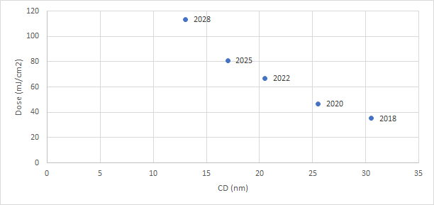
In spite of increasing usage of EUV lithography, stochastic defects have not gone away. What’s becoming clearer is that EUV doses must be managed to minimize the impact from such defects. The 2022 edition of the International Roadmap for Devices and Systems has updated its Lithography portion [1]. An upward trend with decreasing feature size has been revealed (Figure 1).

Figure 1. Increasing EUV doses are projected by the IRDS 2022 Lithography Chapter for decreasing diameter. These plotted doses give photon numbers of 4000-7000 within +/-5% CD of the edge. The photon number is decreasing with decreasing diameter.
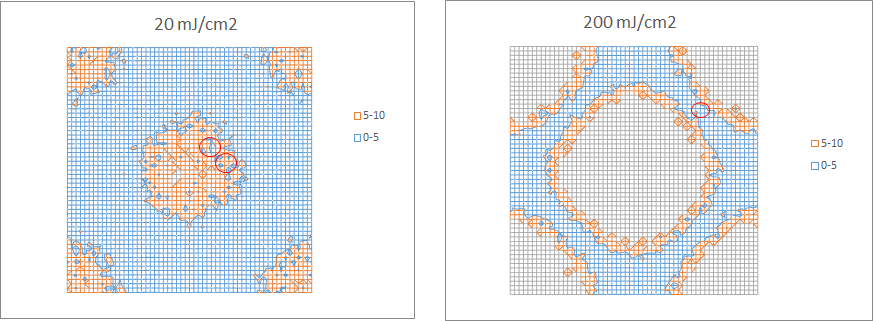
The occurrence of stochastic defects actually defines an EUV dose window [2]. The consequences of going outside this window are shown in Figure 2.

Figure 2. 40 nm pitch contact holes have dose windows defined by the occurrence of stochastics. Too low a dose (left) results in insufficient photon absorption within the target circular area (example: encircled blue spots). Too high a dose (right) results in narrow gaps between features in which bridges (encircled adjacent pixels partly filled with orange) may form due to excessive photon absorption. The pixel size is 1 nm x 1 nm.
Too low a dose results in too few photons absorbed which leads to underexposure-type defects, such as missing, misshapen or undersized contacts. On the other hand, too high a dose results in overexposure-type defects, where gaps between exposed areas are accidentally bridged. From a multitude of studies on this topic, it is understood that the occurrence of defects is minimized (if not completely eliminated) within some range in between the two limits. We may expect that this dose window will shift toward higher values as feature sizes shrink.
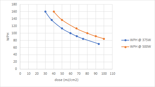
The trend toward higher doses will obviously drive source power toward higher targets [3]. However, even at 500 W, doses going over 100 mJ/cm2 will drive throughput below 100 wafers per hour (Figure 3).

Figure 3. Throughput vs dose, as a function of source power. The calibration is based on Fig. 15 from Ref. 3.
Increasing source power is also an issue for environmental impact. Already EUV machines consume over a MW each [4]. In order to be able pass more wafers per day through each machine, multipatterning may have to be considered [5]. Lower doses would be ok for larger exposed features, but these then need post-litho shrink and have to be packed successively into the tighter pitches, as already practiced with DUV lithography.
References
[1] https://irds.ieee.org/editions/2022/irds%E2%84%A2-2022-lithography
[2] J. van Schoot et al., “”High-NA EUVL exposure tool: key advantages and program status”, Proc. SPIE 11854, 1185403 (2021).
[3] H. Levinson, “High-NA EUV lithography: current status and outlook for the future,” Jpn. J. Appl. Phys. 61 SD0803 (2022).
[4] P. van Gerven, https://bits-chips.nl/artikel/hyper-na-after-high-na-asml-cto-van-den-brink-isnt-convinced/
[5] A. Raley et al., “Outlook for high-NA EUV patterning: a holistic patterning approach to address upcoming challenges,” Proc. SPIE 12056, 120560A (2022).
This article first appeared in LinkedIn Pulse: Where are EUV Doses Headed?
Also Read:
Application-Specific Lithography: 5nm Node Gate Patterning
Spot Pairs for Measurement of Secondary Electron Blur in EUV and E-beam Resists
EUV’s Pupil Fill and Resist Limitations at 3nm
Share this post via:


Solving the EDA tool fragmentation crisis