
Introduction:
The advancements in deep submicron technology and adding multiple functionalities to reduce costs combined with scaling existing operations means that SoC designs become ever more complex. The biggest driving factors to go below the 16nm process node are the decrease in power and the increase in performance due to the higher transistor densities of these advanced nodes. However, doing so creates challenges to physical Implementation and timing/power closure. In particular, high speed IP such as SerDes, DDR, PCIE integration in a large SoC needs careful floor planning to reduce the project time as well as achieve timing/power signoff. In this article, we will look at the new challenges which have been introduced due to 5nm technology as well due to new additional functionality in SoC. We will show the approach to tackle the floor planning and timing issue to reduce the physical implementation iteration.
Methodology
The implementation of large, complex IP integration needs a methodology that efficiently closes the floorplan signoff criteria as well as preventing large timing violations at a later stage.

Challenges of 5nm physical design
A holistic approach is needed to concurrently address the planning, editing and optimization environment for the project along the path from SoC to advanced packaging techniques (like InFo/Feveros/X-Cube). As well as considering the impact backwards up the path of decisions. For example, by iterating the placement bumps, PADs and macros early in the process enables the turnaround time to be reduced.
Another thing to be considered and planned for early in the process are thermal effects long before place and route in order to improve yield and reliability by designing out hot spots that can lead to failures. For example, standard cells packed at high density can create hot spots. This is because, at 14/16 nm nodes, three to four fins are used to provide structural stability to each gate but, below 7nm, two are used. These are higher to compensate for the reduced number of fins and still give the reinforcement required. However, care should be taken with standard cell placement as fins surrounded by dielectric (gate oxide) have poor thermal conductivity and therefore do not dissipate heat as well as expected creating a hot spot. Therefore, doing an early stage of power analysis (Dynamic/Static) helps to prevent hot spot surprises at a later stage at power signoff.
Lastly, process and voltage variation intensity are higher at lower geometries. To combat this, PT-ECO signoff typically needs more than twelve iterations for large complex blocks due to noise and transition requirement.
Challenges of integrating high speed blocks
Partially hardened IP has higher state of flux because of continuous improvement of the hard IP from the analog team. This can be addressed by using models that were tailored for different design stages with increasing level of complexity and completeness as we approach tapeout. Having IP collateral and the list of IP deliverables as soon as possible in the process are vital to a swift and successful integration.
Lastly, design complexity at Floorplanning, DFT integration, Custom Clock tree and timing/power signoff all require scripting knowledge and basic IP understanding to tweak implementation.
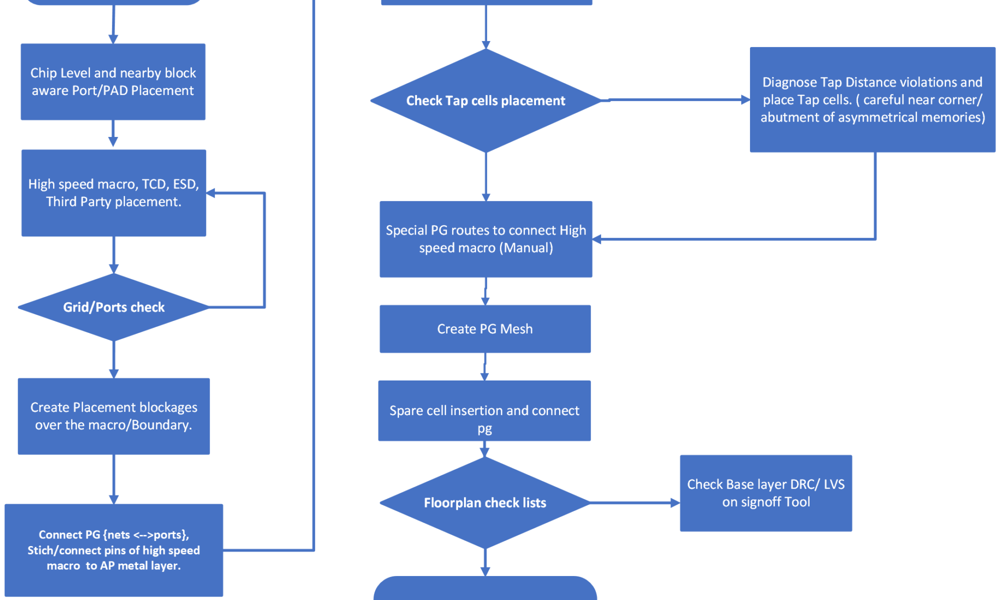
Floorplan Challenges:
On a recent design, the foundry provided a multi-height library and, initially, it was difficult to pass the grid checks. The problem was that we were implementing our design using a power efficient library however the third-party IP was on high performance library. Hence, placement of both library types had to be on least common multiple (LCM) rows.
Things to look out for are:
- Avoiding tap cells and boundary cell insertion on special areas where an analog signal is routing.
- Power Grid (PG) connectivity is important for multiple power domain design along with Analog VDD as well as third party IP VDD.
- Connecting PG nets/pins must be according to guideline defined by the Analog team/Third Party IP deliverables.
- TCD/ESD IP to be connected according to the power clamp implementation rule defined by the foundry.
- Legality checks need to take care of after spare cell insertion: grid check takes care of IP placement legality.
- Integration checks which honor the top-level floorplan DRC (??) while integrating blocks at chip level.
- Terminal/Port placement checks as this is an important check at the initial design integration.
- PG Design Rule Checking (DRC) such as PG Via and power stripe routing, plus macro to macro and macro to boundary spacing rule checks to avoid DRC.
The Floorplanning Goal
This is to have a clean Design Rule Check (DRC) and Layout Versus Schematic (LVS) design that follows the design implementation guideline as well as the timing/congestion aware macro placement.
These are the stages of how to achieve this by improving a floorplan. NB a Synopsys Fusion compiler is used in this example.
I. Grid creation is required due to there being multiple vendors of third-party IP, so generating a grid provides uniformity for interconnection:
create_grid -type block -x_step $cell_site_pitch -y_step $cell_row_pitch -orientations “R0 MX” Macro_wrapper
set_block_grid_references -grid [get_grids Macro_wrapper ] -design Macro_Wrapper
set_snap_setting -class macro_Cell -snap block -user_grid Macro_wrapp
## Macro wrappers need to be snapped to 7.752um, 9.576um which is multiple of cell site 0.051 and cell row height 0.028 (1 track distance)
II. When you do a floorplan, you will need to do manual routing of the high-speed signals. You will need to avoid any placement or routing by creating blockages over the area using
- create_routing_blockage
- create_placement_blockage
For example:
- create_placement_blockage -name $blk_name -boundary [get_attr [get_attr $blk_poly poly_rects] point_list]
- create_routing_blockage -name SNRG#${blk_name} -boundary [get_attr [get_attr $blk_poly poly_rects] point_list] -layers [get_layers -filter full_name!~*G*] -zero_spacing

III. Power Grid (PG) connectivity requires that the PG mesh routing follows the pre-connection command defined by implementation. Hence, we need to connect analog PG ports and BUMP connections along with digital power/ground connectivity.
Example: Connect_pg_net –net VDD [get_pins BUMPS_VDD_*/BUMP]
Connect_pg_net –net VSS [get_pins BUMPS_VSS_*/BUMP]
#Special PG connection
foreach v “VDDA VSSA VDDM” {
Connect_pg_net –net $v [get_pins High_speed_IP_*/[string tolower $v]]
Connect_pg_net –net $v [get_pins Monitor*/[string tolower $v]]
}
IV. Extra signal and special connections as defined by the Analog team to connect at block level can be challenging when you have insufficient or incomplete Library Exchange Format (LEF) but must need to do to check Block level and Chip level Layout Versus Schematic (LVS).
Example:

V. ESD cell and TCD (Test-key Critical Dimension) checks are needed. The electrostatic discharge macro is required to protect high speed analog macros. TCD cells are employed to monitor the critical dimension such as minimum line width, etc. Also check the critical dimension of cells to ensure layout uniformity during fabrication to improve the yield.
Note: We place ESD cells near to Hard IP and supplied the same voltage as that is required by the Hard IP for efficiency.

iii. Terminal/Port placement checks. These are the common and simple checks of floor planning to spot errors.
Example: violation to check.
| Type of Violation | Count |
| Missing Pins | 0 |
| Pin Off Edge | 276 |
| Pins Off Track | 145 |
| Pin Short | 0 |
| Pin Size | 3 |
| Pin Spacing | 3 |
| Total Violations | 427 |
iv. Power Grid Design Rule Checks: Write out PG DRC reports and compare Implementation tool PG DRC with floorplan signoff (rule deck aware) DRC of ICV/Calibre. If DRC violations such as Illegal overlap, insufficient width, minimum metal width min metal area, illegal shapes or min metal edges, try to debug the PG mesh scripts and manual PG via insertion scrips.
Note: Shorts and Opens on the PG should be clean before further executing the next step during the tentative signoff iteration.
In conclusion, Sondrel has been working on advanced nodes for decades and already has several 5nm designs under its belt which were used to create this list of checks and suggestions that can help master the challenges of 5nm design. Further articles can be found at https://www.sondrel.com/solutions/white-papers
Pavan Patel is ASIC enthusiastic physical design engineer. Having implementation and signoff experience of Modem, Camera chip, networking switch, Mobile SoC, Router SoC. Fascinated with VLSI history and impact of SoC on business as well as consumer.
Also Read:
NoC-Based SoC Design. A Sondrel Perspective
Closing the Communication Chasms in the SoC Design and Manufacturing Supply Chain
SoC Application Usecase Capture For System Architecture Exploration
Share this post via:


Comments
There are no comments yet.
You must register or log in to view/post comments.