You could be forgiven for thinking of hearing aids as the low end of tech, targeted to a relatively small and elderly audience. Commercials seem unaware of advances in mobile consumer audio, and white-haired actors reinforce the intended audience. On the other hand, the World Health Organization has determined that at least 6% of people worldwide have at least some hearing loss, and they expect this number to grow to 9% by 2050. Even more remarkably, in the US 20% of people in their 20’s are already reported to have noise-induced hearing loss.
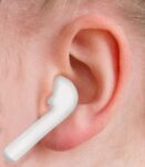
Image courtesy of Jeff Miles
Given the rapid technology and consumerization advances we are seeing in consumer audio, particularly in earbuds, slow progress in hearing aids seems odd since you would think these should share similar growth opportunities. A welcome shift therefore is a recent FDA announcement that Apple Airpods Pro (with an added software feature) is authorized to sell over the counter as a hearing aid. If Apple sees meaningful business expansion in this direction, then I assume other earbud and hearing aid makers will follow quickly.
A different kind of consumerization
In fairness to traditional hearing aid makers there are reasons they didn’t jump on this opportunity immediately. These are partly cost and partly reliability – elderly users on a fixed income don’t want to pay thousands of dollars for devices which may not immediately fit their needs, and they certainly don’t want to upgrade every 2 years.
But more than that, the abundance of features we expect in regular consumer devices can be an active negative for non-tech-aware users, judging by high return rates on early attempts. Such users will certainly enjoy the benefits: increased clarity, TWS support, making phone calls. But don’t ask them to install apps, deal with a bewildering range of options, or figure out what steps to take when something doesn’t work.
This presents a challenge because configuring the aids to a user’s personal hearing needs is critical in making this technology effective. An audiologist can tune a configuration the first time, but hearing needs evolve over time and audiologist visits are inconvenient and perhaps expensive. Even more inconvenient when the aids stop working, especially if you wanted to save money by buying over the counter (OTC).
For this reason, there’s an active trend towards hearing aids self-calibrating through AI, with minimal user feedback. In fact AI-based model opportunities are sparking growth of an early software ecosystem around these devices. According to Casey Ng (Audio Product Marketing Director at Cadence), this 3rd party software market has come as a surprise to some product builders who are not used to the demands of an ecosystem expecting increased memory, APIs, and developer support.
Calibration, or more popularly now personalization, has important value for the rest of us. Wherever we are on the hearing disability spectrum, our ears are unique enough that our hearing experience can benefit from a personalized configuration. This is good news for younger users who need help. Rather than suffer the stigma of wearing classic aids they can use their earbuds (almost a fashion statement these days) which they can optimize to their hearing needs.
Cadence Tensilica Audio DSPs are ready to help
In support of audio applications, the Cadence Tensilica HiFi DSP family offers a range of DSP options from the ultra-low-power HiFi 1 DSP, to the HiFi 5s which is most interesting to me in the context of this hearing aid discussion. This platform is designed to manage TWS, active noise cancellation, also automatic speech recognition for voice-based commands, plus support for more general AI-based applications. Cadence also offers access to a rich supporting audio and voice ecosystem (300 packages) which should accelerate time to market for OEMs.
Among these, noise cancellation options go beyond conventional noise/echo suppression. HiFi 5s offers AI to distinguish and select speech over other audio sources, an important refinement for the hearing impaired.
Importantly these advances (including AI) demand enhanced processing capability. Cadence’s power-efficient HiFi platforms are able to offer that performance yet still extend battery life between recharges, a very important benchmark when users need their hearing aids to last for a complete work-day.”
Casey tells me that the Cadence Tensilica group are also working closely with OEMs who are building their own learning-based personalization models and software. They have also joined a venture with Hoerzentrum Oldenburg GmbH, Leibniz University Hannover, and Global Foundries to build a prototype Smart Hearing Aid Processor (SmartHeAP).
Looks to me like serious commitment to advancing technology in hearing aids! You can learn more about this topic HERE.