The relentless advancement of mobile phone technology continues to push boundaries, demanding SoCs that deliver ever-increasing performance while preserving extensive battery life. To meet these demands, the industry is progressively embracing lower technology nodes with current designs being taped-out at 5nm or below. Designing and verifying clocks at these lower geometries brings mounting complexities and increasing verification challenges. In this rapidly evolving landscape, current clock verification methodologies must be reassessed to ensure optimal clock performance and reliability.
The existing clock methodologies primarily rely on Static Timing Analysis (STA) as a standalone solution or a more advanced approach, that combines STA with a SPICE simulator to analyze critical paths. This flow necessitates the involvement of a CAD department to establish the flow and a strict methodology to produce accurate and timely results, but even then, for an SoC level clock signal at a lower process node, the simulator may lack capacity and/or accuracy requirements. Moreover, the identification of critical paths relies heavily on the judgment and experience of engineers. This approach leads to unnecessary guard-banding, leaving valuable timing margin untapped and limiting overall performance.
At the 7nm, 5nm and 3nm process nodes both the transistor and interconnect dimensions are reduced, resulting in sensitivities to a variety of design and process-related issues, like rail-to-rail failures and duty cycle distortion in the clock signal.
Rail-to-rail Failures
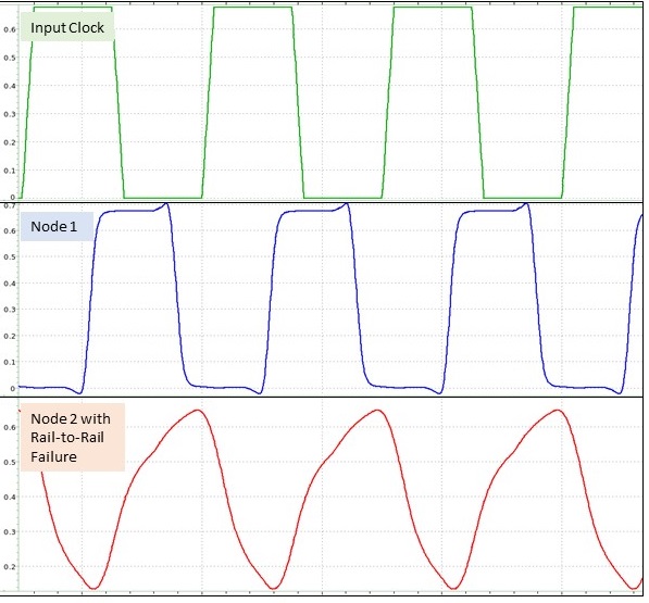
If a clock net has a weak driver, long interconnect and large capacitive loading, then it can lead to increased insertion delays, and worst-case a rail-to-rail failure. The voltage levels on the clock simply don’t reach the VSS and VDD levels in a rail-to-rail failure. Running STA alone will not detect this failure mechanism because STA measures timing at specific voltage thresholds.
An increase in clock frequency reduces clock period, resulting in a shorter time window for the clock to reach the supply rail voltage levels. Voltage scaling also makes the clock signal more vulnerable to rail-to-rail failure, as the smaller gap between the supply and Vth leads to increase in non-linear operation, reducing the drive strength. Even process variations in Vth, transistor W and L variations, or parasitic capacitances will contribute to rail-to-rail failure. Local power supply levels will bounce around from IR drop effects, which then degrade signal levels and timing in the clock signal.

Clock duty cycle distortion
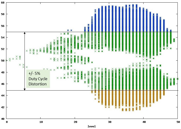
When a clock signal propagates through a series of gates with asymmetric pull-up and pull-down drive strengths, then it causes duty-cycle-distortion (DCD). An ideal duty cycle for a clock is 50% low and 50% high pulse width. Increased clock frequencies can amplify timing imbalances and cause signal integrity issues like DCD. Clock interconnect is impacted by capacitive and resistive effects, which change the slew rate for rise and fall times, delaying the clock and causing asymmetry, making DCD effects more pronounced. Process variations directly alter interconnects, adding imbalances in circuit timing, adding to DCD.

For process nodes with asymmetric PVT corners the DCD becomes more pronounced. Results from a STA tool are focused on insertion delay, so it is less accurate to report DCD and Minimum-Pulse-Width (MPW).
Slew Rate and Transition Distortion
At lower process nodes, the parasitic interconnect has more pronounced resistive-shielding and capacitive coupling, degrading slew rate and clock edge transitions. STA tools use a simplified model for interconnect parasitics which can then underestimate the clock signal degradations.
Power-supply induced jitter
Noise in the Power Delivery Network (PDN) impacts clock timing, producing jitter which impacts clock performance. When the power supply experiences fluctuations or noise, it can introduce voltage variations that directly affect the clock signal’s stability and integrity. Power supply induced jitter can lead to timing errors in clock signals, causing them to arrive earlier or later than expected. This can result in setup and hold violations, leading to potential functional failures in the clock. The increased jitter can also reduce the timing margin, making the design more susceptible to timing violations and potential performance degradation. STA tools primarily focus on analyzing the timing behavior of a design based on a static representation of the circuit and cannot do Jitter. Designers typically use an approximation for jitter effects, so it is really just another guard-band approach.

Topologies using clock grids and spines
Grid and Spine architecture, especially at 7nm and below technology nodes can offer significant advantages including enhanced signal integrity and power and area efficiency. Grid and spine structures provide a regular and structured framework for routing clock signals, reducing the impact of the increased process variations of lower technology nodes, improving signal integrity and mitigating issues like clock skew, jitter and noise. In addition, grid and spine architecture allows for optimized routing of clock signals.
Circuit simulation is the only accurate method to verify grids and spines, but most commercial SPICE simulators do not handle the capacity for such large meshes. Designing a lower technology node clock with grids and spines without an adequate, fast and accurate verification methodology can be a risky proposition.
Summary
Mobile devices require mobile processors, and they often drive the bleeding-edge of IC process technology. Meeting PPA goals in a timely manner is paramount to the success of mobile SoCs. At 7nm and below technology nodes, a fresh approach to clock verification becomes imperative. Failing to adopt such an approach entails increased guard-banding, leading to increased area and power requirements. Most importantly, the conservative nature of guard-banding, leaves valuable performance on the table.
Enter Infinisim’s ClockEdge, an off-the-shelf solution specifically engineered for thorough clock verification and analysis. ClockEdge boasts an exceptional ability to analyze every path within the entire clock domain with SPICE-level accuracy. This has the potential to unlock unparalleled analysis opportunities that are otherwise unattainable using conventional methodologies. Moving to 7nm and below technology node is a costly endeavor, yet it offers significant benefits in Power, Performance and Area (PPA) efficiency. However, guard-banding practices can diminish these advantages. Infinisim’s solution identifies all potential failures and optimizes PPA by minimizing the need for excessive guard-banding, thus capitalizing on the advantages afforded by a move to a lower technology node.
With a well-established reputation, Infinisim has a proven track record in the industry. Their solutions have been adopted as a sign-off tool by their mobile SoC customers, solidifying their position as a trusted partner. Infinisim’s expertise in clock analysis spans a wide range of designs, from 28nm to the most advanced 3nm process node. They provide extensive support for all major foundries, including TSMC, Samsung and GlobalFoundries.
Related Blogs
- CTO Interview: Dr. Zakir Hussain Syed of Infinisim
- Clock Aging Issues at Sub-10nm Nodes
- Analyzing Clocks at 7nm and Smaller Nodes
- Methodology to Minimize the Impact of Duty Cycle Distortion in Clock Distribution Networks
- White Paper: A Closer Look at Aging on Clock Networks
Share this post via:


Comments
There are no comments yet.
You must register or log in to view/post comments.