Bronco Webinar 800x100 1

Layout Migration and DRC Correction at DAC 2012

Layout Migration and DRC Correction at DAC 2012
by Daniel Nenni on 05-20-2012 at 5:00 pm

In the world of sub-40nm IC design, as feature size decreases with each new process node, it becomes increasingly difficult to migrate a layout to a new process technology. Too many factors impact manufacturability and yield. At each new process node, to make sure that a given layout is manufacturable and yields well, it is subject to rules that grow in number, type and complexity. Manual migration of a layout from one process technology to another is extremely complex and time-consuming. When an entire library must be migrated, automation is the only practical choice.

“Today’s 28nm and 20nm technologies present many new and tougher challenges for physical implementation. A library that is competitive from density, routability, reliability and variability perspectives and at the same time respects all new technology design rules is very hard to design manually in a timely manner. Furthermore, frequent changes and updates to new technology design rules make it even more challenging to keep up with manually” explained Coby Zelnik, Sagantec‘s president and CEO. “nmigrate is an automatic layout migration, compaction and optimization solution that is proven to successfully handle all these requirements and updates, delivering optimal results that are design rule clean” Zelnik concluded.

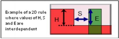
nmigrate is based on innovative 2-D layout optimization technology using dynamic compaction that generates an accurate layout solution optimally satisfying all design rules and constraints. The ability to optimize a layout considering all 2D rules, constraints and cost functions, make it versatile, and suitable for different applications including migration, DRC correction and DFM.

2-D Optimization:The compaction technology allows all 2D rules and effects to be processed in one run, making optimal tradeoffs between constraints and cost in all directions. Including design rules involving multiple shapes where measurement in one dimension influences multiple rule values in the other dimension. Such 2D optimization engine is essential to effectively handle mandatory and DFM rules


Cell optimized for preferred rules: M1 before/after

Self Steering Dynamic Optimization:Advanced technology design rules may have multiple different and discontinuous correct solutions. When polygons and edges start changing position as part of process migration or DRC correction, finding the optimal solution considering all possible discontinuous position configurations is very difficult and requires an engine that can make the right choices and decisions in a multi-dimensional dynamic environment. nmigrate is designed to dynamically evaluate rules and self-steer the engine to achieve the best optimization.

Illustrated are few examples for rules that require dynamic choices and self- steering optimization:

  • Width and common run length dependent spacing rule
  • Contact groups and via array rules where each spacing value depends on the number and spacing of other shapes.
  • Coloring: Due to the printability challenges in 20nm technology new types of rules have been introduced, including DP coloring, A-B spacing rules and auto breaking of odd cycle color conflicts.


Design Rule Changes:
New process technology rules change often as the process matures. Implementing each such change manually is time-consuming and error-prone. nmigrate automates the process and enables quick updates with no time penalty. See below example of a pitch change from 130 to 135nm


Creating Derivative Libraries:With nmigrate, creation of derivative libraries is quick and automated (for example creation of 8-track library from an existing 9-track library).


Full Chip DRC Correction
Often a complete design needs to undergo updates of a few design rules close to tape-out, or even after tape-out for yield enhancement. Similarly, often migrating to a different foundry requires only changing a few design rules. nmigrate uses a fast clip-and-fix flow that is completely scalable by using multiple CPUs.


Applications

  • Process migration
  • Foundry re-targeting
  • Handling design rule changes
  • Creating derivative libraries
  • DFM optimization

Key Features & Benefits

  • Automatically delivers 28nm and 20nm DRC-clean layout using 2D optimization
  • Most optimal results guaranteed by self- steering and dynamic evaluation engine
  • Sophisticated cost function system optimizes layout for yield, variability, reliability and other design metrics
  • Supports user-defined constraints and layout templates

Sagantec is the leading EDA provider of process migration solutions for custom IC design. Sagantec’s EDA solutions enable IC designers to leverage their investment in existing physical design IP and accomplish dramatic time and effort savings in the implementation of custom, analog, mixed-signal and memory circuits in advanced process technologies.

These solutions have been used commercially by tier-1 semiconductor companies, and have been proven to reduce layout time and effort by factors of 3x to 20x and enable dramatically faster introduction of IC products in new technology nodes.

Sagantec has booth #1402at the 2012 Design Automation Conference. See you there!


Going with the Flow at AMD

Going with the Flow at AMD
by Paul McLellan on 05-19-2012 at 11:00 am

At EDPS in Monterey, Tom Spyrou of AMD talked about their compute environment in the context of parallel algorithms. I discovered that they are a big user of RTDA’s FlowTracer so I talked to Philip Steinke at AMD about how they used it.

He said that they largely use it as described in The Art of Flows as a graphical distributed make. They don’t make use of the automatic dependency detection that FlowTracer can do, instead create the dependencies by hand. When one step in the flow completes it declares certain files as outputs, and the next step declares files as inputs. FlowTracer ensures that one step cannot run until the previous ones have completed successfully.

AMD has a large base of users spread throughout the company ranging from fresh graduates to 20-30 years of experience veterans. They have a whole portfolio of different highly automated flows that cover most of the chip design process.

I asked Philip how the flow was originally put together. He told me that it was pretty much like the “French Style” described in the Art of Flows. It is very simple to add new pieces into the flow so that FlowTracer will pick it up and add it to the flow graph.

It was first developed as a solution for a single project, but over time it was adopted by more teams. It is now the basis for almost all digital implementation in AMD.

They have augmented FlowTracer with a couple of other tools. They use LSF (now from IBM since they acquired platform computing late last year) for scheduling jobs on their server farms. And they have created a special in-house utillity for scanning log files looking for error patterns, capable of ignoring errors and so on. This is to deal with the case where a tool doesn’t do so badly that it returns an error status but issues errors that might make the result suboptimal.

Download a free copy of The Art of Flows here.


Novocell Semiconductor Update 2012!

Novocell Semiconductor Update 2012!
by Daniel Nenni on 05-18-2012 at 1:47 pm

Since most of you have not heard of Novocellthis is more of an introduction but they have been around for 10+ years and are NVM (non-volitile memory) pioneers. NVM has evolved into a critical part of the semiconductor ecosystem which is why I sought them out. While SiDense and Kilopass bury each other in legal fees Novocell is doing some very clever things.


NOVOCELL, formerly Intelligent Micro Design, was founded in 2001 and has become the foundation of a growing semiconductor industry in the Pittsburgh region. As a member of The Pittsburgh Technology Collaborative (TTC), Novocell is part of a research network that includes Carnegie Mellon University, Penn State University, The University of Pittsburgh and other TTC member companies.

I had breakfast with the Novocell guys last week and saw them again at the SEMICO IP Ecosystem Conference. I’m a big fan of NVM from my Virage days so you will be reading much more about Novocell on SemiWiki. Here is a description of the Novocell design methodology:

Back at the birth of the antifuse OTP market, David Novosel designed the original NovoBlox OTP memory with the goal of creating one of the most highly reliable memory IPs on the market. It was this goal that gave birth to the unique Smartbit™ bit cell and the many patents Novocell has been awarded over the subsequent years. When developing every product since the initial NovoBlox IP, Novocell’s design team has ensured that the initial standards for “incredible reliability” has never been compromised.

Conscious tradeoffs were made in the design of the initial NovoBlox OTP NVM, specifically trading off size for reliability. Novocell was not driven by creating the smallest memory footprint IP on the market, but we do take immense pride in designing and supplying the most reliable. Since that initial product offering, Novocell has incorporated countless design changes and innovations, some to increase reliability and convenience to customers, and some which have led to smaller area. And, while some competitive memory products may take up less space on an IC in certain configurations, there is no guarantee that those IPs will perform at a par, or better, than Novocell 100% of the time.

To maximize reliability, the breakdown voltage in all Smartbit-based NVM IP is contained entirely within the memory core guaranteeing that only the programmed cells see high voltage. The reliability of unprogrammed cells or other devices on the IC are not negatively impacted with Novocell’s design methodology. Our Smartbit technology also features adynamic(not static, statistically-timed) write protocol withactivesensing which ensures hard breakdown of the gate oxide and the creation of a permanent short between the gate polysilicon and the channel of a programmed device—it’s the foundation of our Smartbit technology, and a feature of our IP that no other antifuse OTP supplier can ever replicate.

You can also visit the Novocell landing page on SemiWiki HERE. Dr. Eric Esteve did a nice blog on Novocell and the NVM market HERE. NVM applications are endless and a very big part of mobile so you will be reading much more about it in the very near future.


Aldec and Tanner EDA at DAC

Aldec and Tanner EDA at DAC
by Daniel Payne on 05-18-2012 at 10:19 am

In April I blogged about a webinar on co-simulation hosted by Aldec and Tanner EDA where they showed how the RTL simulator (Riviera PRO) and SPICE simulator (T-Spice) had been connected together for IC designers wanting to do real AMS simulations.

The availability date of the co-simulation wasn’t clear, so today the press release says that this co-simulation is now available running on either Linux or Windows platforms.

Here’s a screenshot of how you would view both digital and analog waveforms in each viewer:

I found out more info on one product bundle and pricing:

  • Schematic capture, S-Edit
  • Waveform viewer, W-Edit
  • SPICE circuit simulator, T-Spice
  • Verilog-A
  • Verilog-AMS
  • Riviera-PRO for Tanner A/MS
  • $21,083 for a 1 year Time Based License (TBL)

Call you local Tanner EDA sales rep to get more details on pricing for other TBL terms or perpetual licenses.

What makes this particular combination of AMS simulation different is how affordable it is, compared to what the big three EDA companies are charging.

If you are headed to the DAC show in San Francisco held June 4-6, then check out this co-simulation at Aldec booth #2126 or Tanner EDA booth #1126. You can even register online for a private demo at Tanner EDA.


CDN Live in Munich: Cadence is back on track!

CDN Live in Munich: Cadence is back on track!
by Eric Esteve on 05-18-2012 at 3:44 am

Before going to Munich to attend to CDN-Live, I took a look at the agenda to figure out which presentations to attend, and I must say it was not so easy to choose: CDN Live agendais dense, with multiple tracks running in parallel (Custom Design, Digital Implementations, Design IP, Functional Verifications and Verification IP, PCB design… and more) and presentations given by Cadence, by partners like Global Foundries, IMEC, ARM, or Universities and by Cadence’s customers, TI, Renesas, NXP, ST-Ericsson to name a few.

The first part of Tuesday started with a 30 mn talk from Lip-Bu Tan, the CEO of Cadence who has joined the company three and half years ago to put the company back on track and this was a real challenge as, before his venue, Cadence was about to lose credibility (and soul), due to some weird accounting approaches. I don’t know much about it, just that the technical community, inside and outside the company, was confused. Then, at the beginning of 2010, came “EDA 360” initiative. To summarize, EDA 360 reflect the vision about the future of Electronic design, it says that supporting H/W design only is not enough, and that large EDA companies will have to offer the right tools to manage H/W and S/W development, design verification and system validation. Because this vision was proposed with a superb marketing campaign, it generated high expectations, and finally some deception… By definition, a vision reflects a long term view of where you want to go within, say, 10 years, not the company’s product port-folio today or even tomorrow (next year). So, I was pretty impatient to listen to Mr. Lip-Bu Tan, and to know what were the key messages delivered by Cadence management!

The show took place in an amphitheatre; the ten meters high backdrop of the stage was made of multiple LED panels changing color (depending on the speaker) – a classic EDA show. Then Mr. Lip-Bu Tan started talking: about Cadence, putting the focus on Cadence technical community excellence (which is true, according with my own experience when running technical discussion with product marketing person from the company). Talking also about Cadence’s customers, saying that the company want to serve them well, even when their demand is challenging, adding that he is travelling a lot to meet them. You can argue that it’s easy telling, but the message itself is very positive.

Mr. Lip-Bu Tan also said that he is a VC, and as being involved as an investor with various Electronic companies worldwide, he tries to make sure that, first they use Cadence tools, second that they can get the higher satisfaction from the tools, which means for Electronic companies, release a product at spec and reach their time to market objectives. I must say that I completely buy such an argument! When the CEO is also a customer for the products sold by the company he is running, this should increase the level of confidence customers may have in the company.

Another word was part of the message: “humble”. I heard it the day before the show, from a Cadence employee talking about the CEO. I also heard it from the CEO during the show, when he said that this should be the behavior of Cadence employees when dealing with customers. You may think this is easy telling again… Maybe, but some of the EDA industry representatives have been known for their… arrogance in the past, then, indicating the opposite direction should be positively perceived by Cadence customers!

Because he presented himself as a VC, Mr. Lip-Bu Tan was smart enough to leave the highly technical content to the next person on stage, Tom Beckley (Sr VP, R&D, Custom IC and Signoff, Silicon realization Group). I will not go into the details of this presentation, as EDA tools development is not my area of expertise. I would like to mention that Tom has specially thanks Jacques-Olivier Piednoir, who I know since my very first job in Matra Harris Semiconductor, and who has helped me a lot, back in 1986, to prepare my first trip in the Silicon Valley to present a paper at the 3[SUP]rd[/SUP] Multilevel Interconnect Conference (multilevel was meaning the second metal level, for a 2 micron technology, at that time!). And because we are leaving in a small world, I should mention that Jacques-Olivier has worked under the direct responsibility of Paul McLelan, it was in the 80’s at VLSI Technology!


The show ended with a very informative Industry keynotes from Luc Van den Hove, CEO of IMEC, dealing with the various prospective developments in CMOS technologies, like:

  • Enabling lithography: 193nm immersion litho (incl. double patterning), EUV litho
  • New materials in devices: high-k, strained Si
  • New device concepts: 3D, FINFET, tunnelFET
  • Advanced memory: DRAM, floating gate, resistive RAM
  • Advanced interconnect: 3D, Cu/low-k

Then, the conference started, with multiple tracks taking place in smaller rooms. I have just attended a few presentations about DDRn Controller and WideI/O IP, both very technical and certainly useful for the design community. If I have to give an evaluation, I would say 85% technical and only 15% (or less) marketing. I told you, Cadence want to pass the message that the company has renewed, focus on the technical content and tell their customers that they want to serve them well… as a customer, that’s the kind of message I like to hear! Yes, I had a free lunch, but no, that’s not the reason why I write this way…

Another blog will be fully dedicated to their NVM Express subsystem IP product launch, happening during CDN Live, which could be a very interesting move on the (IP and VIP) chess game currently running between Cadence and Synopsys… stay tuned!

Eric Estevefrom IPNEST


Intel is Selling Itself Short on Trigate!

Intel is Selling Itself Short on Trigate!
by Ed McKernan on 05-17-2012 at 9:15 pm

Perhaps the most pertinent comment raised by an analyst at Intel’s Investor Forum last week came from Dan Hutcheson of VLSI Research to Brian Krzanich, the COO and head of global manufacturing and supply chain. He said: “I think you sold yourself short on Trigate, the benefit of fully depleted vs. planar and the impact on leakage.” The answer is, of course, yes. This, though is confusing to the Wall St. crowd since they don’t have an idea of how process technology, processor architecture and circuit design can be married in a precise way to target various market segments. Trigate’s ability to shut off leakage has taken away the one advantage ARM has for itself in the battery life wars. If I can be bold, Trigate is the biggest thing to occur in Mobile and Server computing in the last 10 years… maybe longer.

Wall St. Analysts meet at the same water hole reciting the common lingo: ARM is low power, bring out the Intel Dead, Arm is low power, bring out the Intel Dead, ARM is low power, bring out the Intel Dead! It is so predictable and trite that it could be set to the cadence of a Monty Python scene. OK, I’ll move along…but Intel isn’t Dead yet.

Unlike Mr. Hutcheson, though, Wall St. analysts are not clued into the fact that in the new mobile world it is not about the instruction set or that past performance is a definitive predictor of future results. Instead it is about mobile processors that can handle three modes of operation efficiently. The first is a sprint mode, where the processor reaches for its highest MHz for a short period of time in order to bring up new applications in a snappy manner. The second is to offer a cruise mode where voltage and frequency are tuned to a low frequency to run things like video efficiently and without dropping frames. Finally there is standby where you want to be as close to 0mW as possible, even between keystrokes. Depending on the user, any of the modes can be dominant in the battery life equation. However, if you are like most users, you are idle 99% of the time. Therefore standby power becomes critical.

The standby mode is where ARM has always had a big advantage. Intel’s Trigate 22nm process cuts off the leakage and enables the processor to drop into a standby voltage of 0.7V. This is a major milestone in low power operation. It is still true that Intel has work to be done in the area of a more efficient circuit design on the next Atom architecture. It is there that the full realization of Trigate gets embedded in Intel’s mobile cores – Atom and Haswell.

If you talk to an Apple engineer, you will understand that a major part of their efforts in designing their mobile processors is in running a multitude of voltage supply planes across the chip in order to cut off power to blocks that are idle or to run one block at a lower voltage and lower frequency than another. Essentially squeezing power is the name of the game. With Trigate, the hundreds of circuit design engineers that are assigned to each of the Intel mobile cores will merrily go about slicing and dicing up the functions on much lower operating voltage ranges. There may end up being an x86 core running at one dynamic voltage and frequency range while another runs at a much lower frequency and voltage. Workloads than will be directed to that which is best able to do the job most efficiently. Ditto the above for Server Processors with even more cores.

The era of brute force high MHz processors has been over for some time and Intel was caught by surprise on the ramp up of smartphones and tablets. The process guys though, in the end, always seem to bail them out of a jam. This time though, it is not just one process node of density improvement, it is a shift in the operating voltage down and to the left (towards ZERO Volts or First to Threshold), that will provide incredible, measurable improvements across all mobile markets.

FULL DISCLOSURE: I am long AAPL, INTC, ALTR, QCOM


Semiconductor Ecosystem Keynotes: ARM 2012

Semiconductor Ecosystem Keynotes: ARM 2012
by Daniel Nenni on 05-17-2012 at 5:00 pm

Yesterday’s SEMICO IP Ecosystem Conference was well worth the time. Everybody was there: ARM, Synopsys, Cadence, Mentor Graphics, GlobalFoundries, TSMC, MIPS, Tensilica, AMD, Atrenta, Sonics, and Tabula, everybody except Intel of course. What do Intel and I have in common? We don’t play well with others…

First up was Jim Feldham, President of Semico Research with some interesting industry forecast slides. Semiconductor revenue grew 1.3% in 2011 and is predicted to grow 9% in 2012, very believable, even with 28nm wafer allocation. Tablets (+46%) and Smartphones (+34%) lead the way with the SoC market reaching $85B. I agree with this assessment 100%.

Second up was Warren East, ARM CEO. I like Warren, he is a humble man (like me) and has the traditional British dry sense of humor (unlike me). Warren’s presentations pack the most content you will see from a semiconductor CEO. Since ARM owns 99.99% (exaggeration) of the mobile business their customer surveys are very relevant. Here are some interesting takeaways from Warren’s slides:

  • 5B+ People Connected
  • $10 Mobile Phones
  • Mobile Devices Outsell PCs
  • Always On, Always Connected

Warren didn’t mention “He who must not be named” (Intel) but clearly this is a clean shot at them:

  • Fabless Model Lowers Costs
  • IP is Key: 100+ Blocks Per Chip
  • $200M Cost for 14nm SoC
  • Design Costs = 52.8% Software + 47.2% Hardware
  • Standards Reduce Costs

Taking a “systems” view:

  • A vibrant ecosystem is maintained through collaboration and aligned investments
  • Tweaks to current models will not solve big challenges or drive significant growth
  • Boundaries will need to shift and change, enabling broader IP and services that spread development costs across the chip ecosystem

Bottom line: It’s all about the ecosystem. Linaro is one example as I blogged in Intel Versus ARM (Linaro).

The SoC Design community is dedicated to design engineers developing highly integrated system-on-chip solutions with ARM technology. This site addresses every phase of SoC design, from architecture selection through front end design and back end implementation and manufacturing. Learn more about best practices for designing advanced SoCs based on ARM Cortex processors, Artisan physical IP, CoreLink system IP and ARM Connected Community IP, tools and services.

ARM has a landing page on SemiWiki now which you can find HERE, ARM related blogs are organized there. The theme you will notice is ecosystem and SoC. SemiWiki blogger Don Dingee has a series of blogs on Smart Mobile SoCs including NVIDIA, Apple, Samsung, TI, and Qualcomm. He even did one on Intel: Smart Mobile SoCs: Intel. Don will go to China for the next one so stay tuned!


Smart mobile SoCs: Intel

Smart mobile SoCs: Intel
by Don Dingee on 05-16-2012 at 3:59 pm

Talk about an unusual position. Intel finds themselves very much currently outside when it comes to mobile SoCs for phones and tablets. After several attempts at soul-searching and a true understanding of the term “low-power” (not meaning 3W, but instead < 1W), they finally have a part – in the form of “Medfield”, aka the Atom Processor Z2460 – that can technically compete for business while their roadmap develops. Continue reading “Smart mobile SoCs: Intel”


CEVA is the undisputed DSP worldwide leader

CEVA is the undisputed DSP worldwide leader
by Eric Esteve on 05-16-2012 at 10:54 am

Anybody working in the wireless handset segment probably knows that CEVA is the provider of DSP IP cores, and if you are simply a wireless handset user, you should know that the baseband digital signal processing is the function allowing your phone to process the RF (analog) signal coming from the outside world. If you have been involved in the wireless segment before 2002, you may remember a company named DSP Group: the merge of the IP licensing division of DSP Group and Parthus has been named CEVA, and CEVA has enjoyed 90% market share for DSP IP products in 2011, according with the Linley Group. A 70% market share simply means that CEVA’ DSP IP have been integrated into 1 billion IC shipped in production in 2011!

Some of you may remember that, during the 90’s, when the wireless phone segment has been created from nothing, to emerge in 1995 and sky rocket in the 2000, the baseband processing was digital (by opposition of the very expensive but low sound quality analog wireless) and one company was dominating the IC market: Texas Instruments, thanks to their DSP. Initially, the handset made by Ericsson where even using the TMS320 DSP standard products from TI, before TI was pushed to propose a DSP core, which could be integrated into a more complex ASIC. But this was not a DSP IP core. In other words, Ericsson, Nokia, Alcatel and so on had to develop their devices, using TI ASIC technology, and TI fabs. At that time, it was seen as a very good strategy by TI: they had architecture a new DSP specially tailored for the wireless handset application and this core was the hook allowing to fill the fab with the devices which will eventually become application processor later on, except that, at that time, most of the processing power was in the DSP and the processor core was… an ARM 7!

When DSP Group (CEVA today) came on this market, TI competition (VSLI Technology, STMicroelectronics and more) was certainly happy as they could propose an alternative solution to the Nokia et al., but it took some time before these OEM decide to move the S/W installed base from TI DSP to CEVA DSP IP core, that they had to do if they decide to move from TI to another supplier. It was a long route, but when you consider the 1 billion devices integrating a CEVA DSP IP, this means that (probably) 800 million of the 1,500+ million of wireless handset shipped in 2011 uses CEVA DSP, the remaining devices addressing a broad range of applications including cellular baseband, imaging, vision, audio, voice, voice-over-IP and more. In term of architecture, it was also a long route: if in 2000, it was possible to use a simple DSP IP core to support the baseband processing, today’s communication standards including LTE-Advanced, LTE and HSPA+ are supported by CEVA-XC4000 architecture, offered in a series of six fully programmable DSP cores, running at speed up to 1 GHz, as you can see on the above picture.

The market share numbers (once again, 70%, a magic number for an IP vendor!) were published in The Linley Group’s recent report, titled ‘A Guide to CPU Cores and Processor IP’, and have been commented by one of the co-author: “CEVA continues to be the most successful supplier of DSP IP — its licensees shipped more than one billion chips in 2011,” said J. Scott Gardner, an analyst at The Linley Group. “CEVA has an impressive customer base for its DSP portfolio, especially in communications and multimedia. Furthermore, with the 4G transition well underway, high-performance programmable DSPs are required to efficiently handle complex multimode baseband processing. CEVA is well positioned to capitalize on this trend.”

The next comment, from the CEO of CEVA, is reflecting the satisfaction of being the market leader with 70% market share, and I am sure I would have the same behavior, would I be in this position!

“CEVA is pleased to be ranked yet again as the worldwide leader in DSP IP by The Linley Group,” said Gideon Wertheizer, CEO of CEVA. “Our unrivalled expertise in DSP technology for high volume mobile and digital home applications drives our success and is the reason we are the DSP-of-choice for many of the world’s leading semiconductors and OEMs.”

CEVA is also proposing Controller IP for SATA and SAS, we will come back to these IP in another blog. The focus of today was DSP IP core, and, like ARM IP core is coming in mind immediately when you consider a wireless handset phone or smartphone, CEVA DSP IP is the dominant solution for the same. Just a final remark: CEVA is claiming to be the only Israeli company who’s product is integrated into the Apple iPhone, if anybody knows what product CEVA has sold to Apple (I strongly guess that Apple does not allow their supplier to communicate about this), feel free to put a comment, or to send me a note.

Eric Esteve from IPNEST –


Analyzing Cortex Performance

Analyzing Cortex Performance
by Paul McLellan on 05-16-2012 at 7:45 am

CPAK sounds like something politicians create to collect money, but in fact it is a Carbon Performance Analysis Kit. It consists of models, reference platform, initialization software (for bare metal CPAKs) or OS binary (for Linux and Android based CPAKs). They are (or will soon be) available for ARM Cortex A9, ARM Cortex A15 and ARM big.LITTLE (which is an A15 and an A7).

Designing a complex microprocessor-based system, especially a multi-core one, has two major challenges:

  • getting the software written and debugged
  • analyzing the system performance for speed, power and unanticipated bottlenecks

CPAKs primarily address the second problem: what clock-rate do I need to use? how many cores? is my cache big enough? does my bus fabric work as advertised? Since source code is included for all of the software provided with the CPAK, it can also get you up and running quickly from the software side too, eliminating the need to figure out how to initialize all the system components.

A CPAK saves weeks or months in time to market by providing an off-the-shelf reference platform complete with all the software to bring them up. So users can start analyzing, optimizing and verifying performance of ARM processor-interconnect-memory subsystems within minutes. The platforms can further be customized using the Carbon IP Exchange model portal.

A CPAK contains fully cycle-accurate models and so can be used for this sort of detailed performance analysis. Fast models, which are great for software development, only have rudimentary performance analysis and are not accurate enough for system architecture work.

Bare metal CPAKs are free of charge (you need to have Carbon SoC Designer Plus to be able to use it though). Other CPAKs have a one-time fee.

CPAKs will also work with Swap & Play. This means that you will be able to boot the operating system with a fast model (without it being accurate enough to do any detailed analysis) and then switch out the fast model for a cycle accurate model to analyze the performance of the system doing something more interesting than running its bootstrap.

The CPAK family for ARM Cortex Processors will be available in bare metal and Linux configurations in Q2 and in Android configurations in the second half of the year.

Come and find out more at DAC. Carbon will be in the ARM Connected Community Pavilion, booth 802, and in their own booth 517.