You are currently viewing SemiWiki as a guest which gives you limited access to the site. To view blog comments and experience other SemiWiki features you must be a registered member. Registration is fast, simple, and absolutely free so please,
join our community today!
A modern fab can cost as much as $10B dollars. That’s billion with a B. Since it has a lifetime of perhaps 5 years, owning a fab costs around $50 per second and that’s before you buy any silicon or chemicals or design any chips. Obviously anyone owning a fab had better be planning on making and selling a lot of chips if they are going to make… Read More
A Brief History of FPGAsby Daniel Nenni on 08-26-2012 at 7:30 pmCategories: FPGA
From the transistor to the integrated circuit to the ASIC, next comes programmable logic devices on the road to the mainstream fabless semiconductor industry. PLDS started in the early 1970’s from the likes of Motorola, Texas Instruments, and IBM but it wasn’t until Xilinx brought us the field programmable gate array (FPGA)… Read More
AMS Programmable Prototype Platformsby ahmed.shahein on 05-21-2012 at 10:25 amCategories: Aldec, EDA, FPGA
AVNET released their 15[SUP]th[/SUP] Xfest this year, a couple of months ago. It was here in Germany last week. It was a well organized event, rich with invaluable technical information and full of decent smart engineers and managers. If you missed it this year register for the next event as soon as you can.
It was a very successful… Read More
Oasys announced that it closed its series B funding round with investments from Intel Capital and Xilinx. The fact that any EDA company has closed a funding round is newsworthy these days; companies running out of cash and closing the doors seems to be a more common story.
Oasys has been relatively quiet, which some people have taken… Read More
EDPS: SoC FPGAsby Paul McLellan on 04-09-2012 at 4:00 amCategories: Events, FPGA
Mike Hutton of Altera spends most of his time thinking about a couple of process generations out. So a lot of what he worries about is not so much the fine-grained architecture of what they put on silicon, but rather how the user is going to get their system implemented. 2014 is predicted to be the year in which over half of all FPGAs will… Read More
As many analysts have noted, it is difficult to imagine what Intel’s foundry business will look like one, two or even three years down the road because this is all new and what leading fabless player would place their well being in the hands of one who is totally new at the game. I would like to suggest there is a strategy in place that will… Read More
When process nodes reached 28 nm and below, it appeared that design density is reaching a saturation point, hitting the limits of Moore’s law. I was of the opinion that the future of microelectronic physical design was limited to 20 and 14 nm being addressed by technological advances such as FinFETs, double patterning, HKMG (High-k… Read More
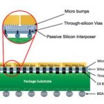
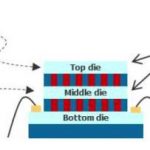
The IEEE has an Orange Country Chapter of the Components, Packaging and Manufacturing Technology Society who are organizing an all-day workshop, 3D Integrated Circuits: Technologies Enabling the Revolution. This looks to be an informative day with real-world examples in both design and test being presented by over a dozen … Read More
The “old saw” is “To Sell in May and Go Away.” It’s a Maxim that particularly applies to semiconductor stocks as they typically drop from a post April earnings peak through the summer doldrums to a late September nadir only to be revived in the prelude of October earnings. It has happened again this year, although the path taken by the… Read More
Intro
My first exposure to hardware prototyping was at Intel back in 1980 when the iAPX 432 chip-set group decided to build a TTL-based wire-wrap prototype of a 32 bit processor to execute the Ada language. The effort to create the prototype took much longer than expected and was only functional a few months before silicon came back.… Read More