You are currently viewing SemiWiki as a guest which gives you limited access to the site. To view blog comments and experience other SemiWiki features you must be a registered member. Registration is fast, simple, and absolutely free so please,
join our community today!
Intel’s new Tri-Gate technology is causing quite a stir on the stock chat groups. Some have even said if Intel uses its Tri-Gate technology on only Intel processors ARM will be in deep deep trouble. These guys are “Intel Longs” of course and they are battling “Intel Shorts” with cut and paste news clips.
“ARM is in trouble & this… Read More
At DAC 2011 in San Diego, Apache gave many product presentations. Of course not everyone could make DAC or could make all the presentations in which they were interested. So from mid-July until mid-August these presentations will be given as webinars. Details, and links for registration, are here on the Apache website.
The seminars… Read More
During last week-end, I had the good surprise to meet with one of my oldest friend, Eric, who remind me the old time, when we were working together as ASIC designers for… a Supercomputer project.
In France, in a French company (Thomson CSF) active in the military segment and being able to spend which was at that time a fortune ($25M) … Read More
In my rush on Wednesday at DAC I had almost over-looked the last two companies I talked with: Invarian and AnaGlobe. These last two I had hand-written notes on paper, so I just got to the bottom of my inbox tonight to write up the final trip reports.
Invarian
Jens Andersen and Vladimir Schellbach gave me an overview of tools that perform… Read More
We all knew that Apache had filed for an IPO earlier and were just waiting for the timing and price to be revealed. Rumors have been circulating about an acquisition and today we know that the rumors were true asAnsys paid $310 million in cash for Apache.
Ansys stock has surged some 35% over the past twelve months:
Products
This acquisition… Read More
SOC Realizationby Paul McLellan on 06-27-2011 at 5:28 pmCategories: EDA
There are some very interesting comments to the last entry on SoC Realization and how more and more chips are actually assembled out of IP. There was clearly a lot of discussion in this area at DAC, although most people (Atrenta being an exception) don’t use the term SoC Realization, presumably because it was originated by … Read More
Introduction
Before DAC I met with Stephen Pateras, Ph.D. at Mentor Graphics, he is the Product Marketing Director in the Silicon Test Solutions group. Stephen has been at Mentor for two years and was part of the LogicVision acquisition. He was in early at LogicVision and went through their IPO, before that he was at IBM in the mainframe… Read More
OpenAccessby Paul McLellan on 06-21-2011 at 1:11 pmCategories: EDA
Probably everyone knows that openAccess is a layout database. It was originally developed at Cadence (called Genesis) but has since been transferred to Si2. Strictly speaking, openAccess is actually an API and the database is a reference implementation. The code is licensed under a sort of halfway to open-source: you can use … Read More
Can Your Router Handle 28 nm?by Beth Martin on 06-20-2011 at 7:11 pmCategories: EDA, Siemens EDA
With the adoption of the 32/28 nm process node, some significant new challenges in digital routing arise—including complex design rule checking (DRC) and design for manufacturing (DFM) rules, increasing rule counts, very large (1 billion transistor) designs. To meet quality, time-to-market, and cost targets, design teams… Read More
Intro
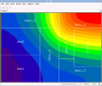
Massimo Sivilotti, Ph.D of Tanner EDA showed me their 3D field solver in the HiPer PX extraction tool at DAC last week.
Notes
Tool Suites – schematics, layout, SPICE simulation, DRC/LVS
– HiPer PX: 3D Field solvero Layers, dielectrics,
o Finite element analysis
o Boundary element methods
o 2D mode for pattern matching… Read More