There’s this EDA company. They have over 100 tapeouts. They have a $28M in funding. They have 250 people. And you’ve never heard of them. Or at least I hadn’t.
They are ICScape. They started in 2005 with an investment from Acorn Campus Ventures and delivered their first product, ClockExplorer, in 2007 and their second, TimingExplorer in 2009. They then have gone on to develop a complete openAccess-based place and route system including placement, clock-tree-synthesis, routing, static timing analysis, parasitic extraction and…
In 2008-2010 during the technology downturn they survived purely on product revenue. They turned their attentions to China, which was one area that was still buoyant. Also in China is a 20 year old EDA company called Huada Empyrean Software (HES) who have an openAccess-based analog environment. HES is a subsidiary of China Electronics Corporation, China’s largest electronics conglomerate (and an SOE). HES want to expand outside of China and become a global player, so it was spun out of CEC and merged with ICScape and provided with $28M in funding. They have one engineering organization. HES sells the whole product line in China and Taiwan. ICScape everywhere else (the US, Korea and Japan today, and Europe soon).
They have big plans to become a big global EDA player. I have no idea how good their technology is but they claim that over 100 chips have been taped out, including some at the 28nm technology node, so it should be pretty solid. Customers include Marvell, Huawei, ZTE, NHK and more.
 The SoC product line is based around accelerating design closure by reducing the number of iterations by 50%. It consists of four tools:
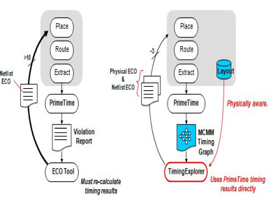
- TimingExplorer, a physically aware multi-corner, multi-mode timing ECO tool
- ClockExplorer, which can reduce clock insertion delay by up to 50% and clock-tree power by 40%
- Skipper, a high-performance and ultra-large capacity chip finishing solution
- FlashLVL, a high-speed layout comparison tool
The analog product line is now in its 6th generation. It is focused on big-A small-D designs with lots of analog and limited amounts of digital. It contains:
- interconnect-aware layout editing
- high-capacity parallel circuit simulation
- hierarchical parallel physical verification
- mixed-mode, multi-corner parasitic extraction and analysis
Going forward the plan is to bring all the technologies together, which is not such a daunting task as it might be since both product lines are native OA-based. At the same time expand their channel to have complete coverage everywhere.
Share this post via:


Solving the EDA tool fragmentation crisis