
I was asked to present at Nikon’s LithoVision event again this year. LithoVision is held the day before the SPIE Advanced Lithography Conference also in San Jose. The following is a write up of my talk.
The outline of the talk is:
- NAND – scaling with layers
- DRAM – peripheral scaling and new options
- Logic – high performance and Internet of Things
- Conclusion
NAND Scaling With Layers
3D NAND has now passed 2D in bits shipper year and is rapidly becoming the dominant form of NAND Flash memory. 3D NAND has switched NAND scaling form being lithographically driven to deposition and etch driven by stacking layers.
Figure one present the TCAT Process that is used by Samsung and Toshiba, the two largest producers of 3D NAND.
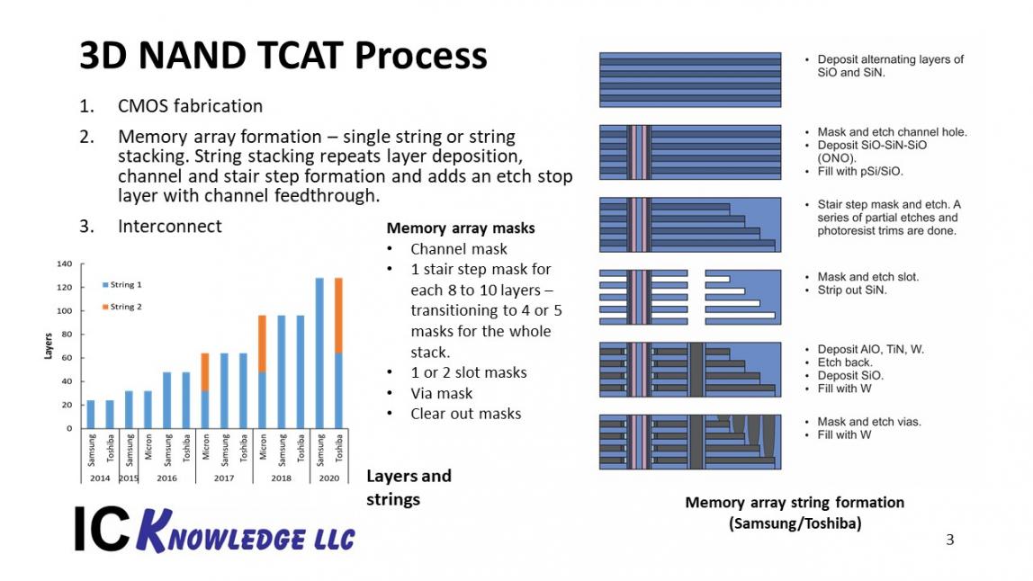
Figure 1. 3D NAND TCAT Process.
In 3D fabrication there are three main segments:
[LIST=1]
The memory array string formation sequence is:
- Deposit alternating layers of oxide and nitride. This is a gate last process such and Samsung and Toshiba both use. Intel-Micro deposit alternating layers of oxide and poly silicon.
- The channel hole mask is applied and etched down through the stack. The channel hole is filled with an Oxide-Nitride-Oxide (ONO) film and then a poly silicon channel filled with oxide. This etch is very challenging particularly for oxide/poly and that is why Intel-Micro have gone to string stacking earlier than Samsung or Toshiba.
- A thick photoresist is applied and patterned with the stair-step mask. An etch and shrink sequence is used to create a set of stairs. Approximately 8 stairs can be created before the mask has to be stripped off and a new mask applied. A 64-layer device typically requires 8 masks to fabricate the entire stair case.
- A slot mask is applied and etched down through the stack. A wet etch is used to etch out the nitride layers that are then replaced with aluminum oxide and titanium nitride memory cell films and then the horizontal layers are filled with tungsten. The tungsten is etched back in the slot, oxide is deposited, and the trench is filled with tungsten. There may be a second shallow slot as well.
- The via mask is now applied and etched down to the stair steps.
- Clear out masks may be required prior to channel and slot masks because the hard mask and layer stacks are hard to align through. A clear out is a large area square etched down through the layers to expose alignment targets.
The graph in the bottom left of the figure illustrates string stacking by company. Intel-Micron began string stacking at 64 layers, Toshiba is expected to string stack at 128 layers and Samsung is expected to produce 128 layers as a single string.
In figure 2 the mask counts for 3D by company are shown:
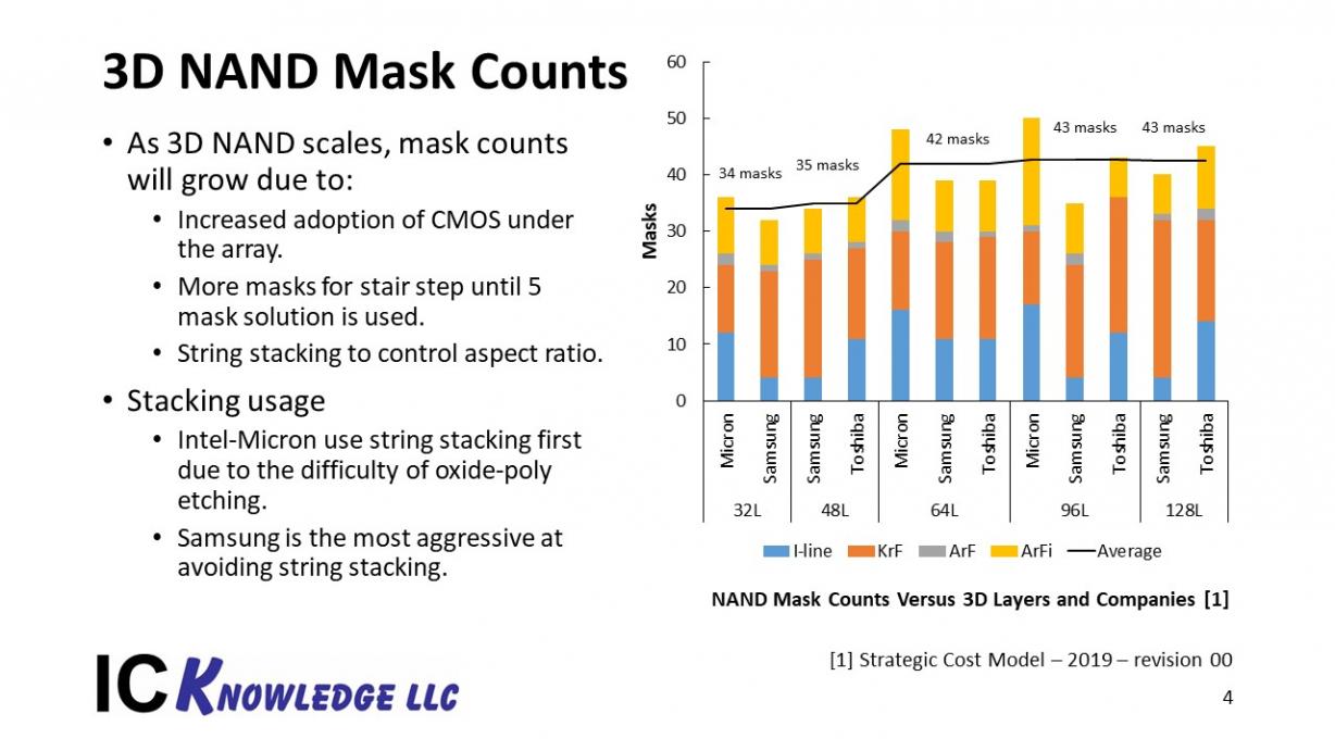
Figure 2. 3D NAND Mask Counts
There are a couple of competing trends going on here. String stacking and moving some of the CMOS under the memory arrays increase mask counts, while simplified stair steps schemes using less masks reduce mask counts.
In figure 3 the NAND bit density by year is presented.
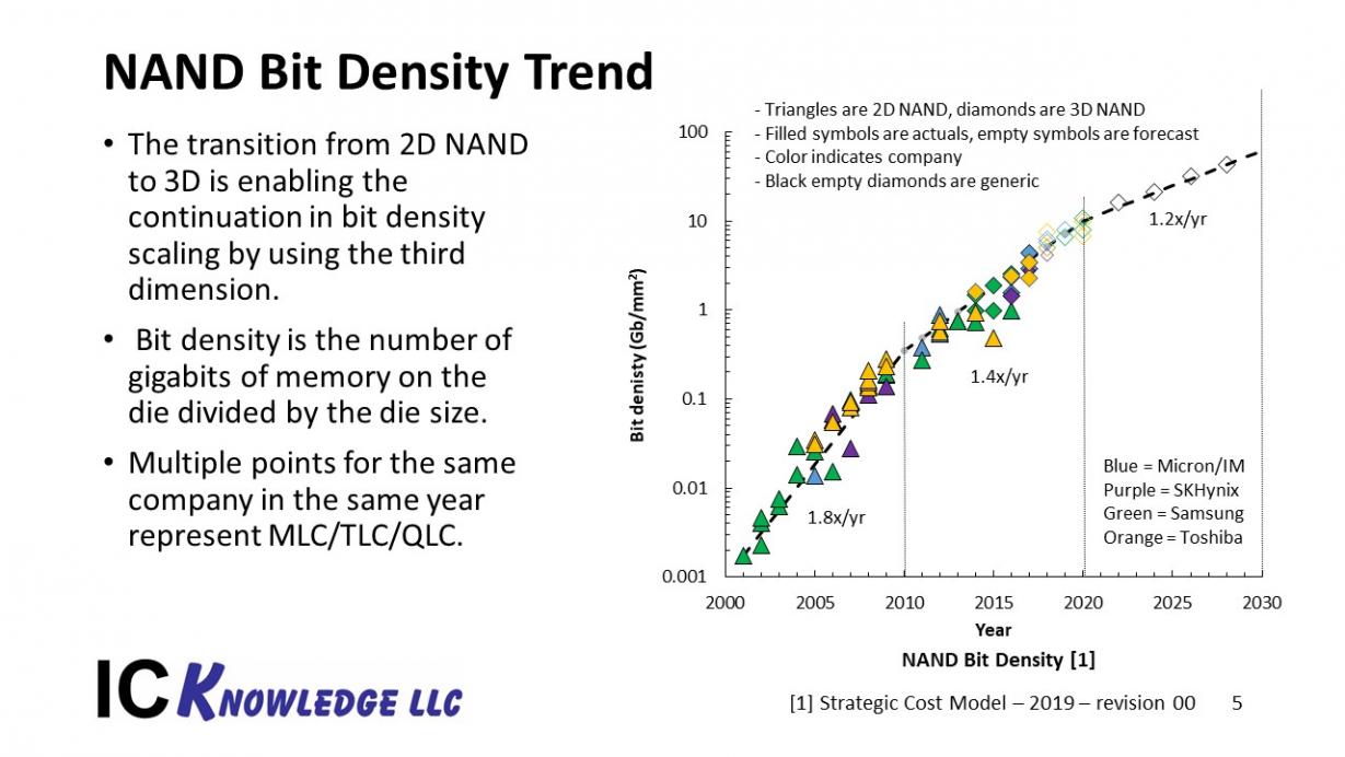
Figure 3. NAND Bit Density Trend
From 2000 to 2010 2D NAND lithography driven scaling was providing a 1.8x/year increase in bit density. After 2010 2D NAND lithographic driven scaling slowed down due to device scaling issues and bit density growth slowed to 1.4x/year. In the mid-2010s 3D NAND was introduced and continued the 1.4x/year scaling trend for the rest of the decade. In the 2020s we are forecasting further slowing of scaling to 1.2x/year due to the challenges of fabrication such tall memory stacks.
DRAM Peripheral Scaling and New Options
DRAM scaling has been facing fundamental challenges trying to scale down the capacitors and peripheral scaling has become a key contributor.
Figure 4 illustrates DRAM node scaling by company.
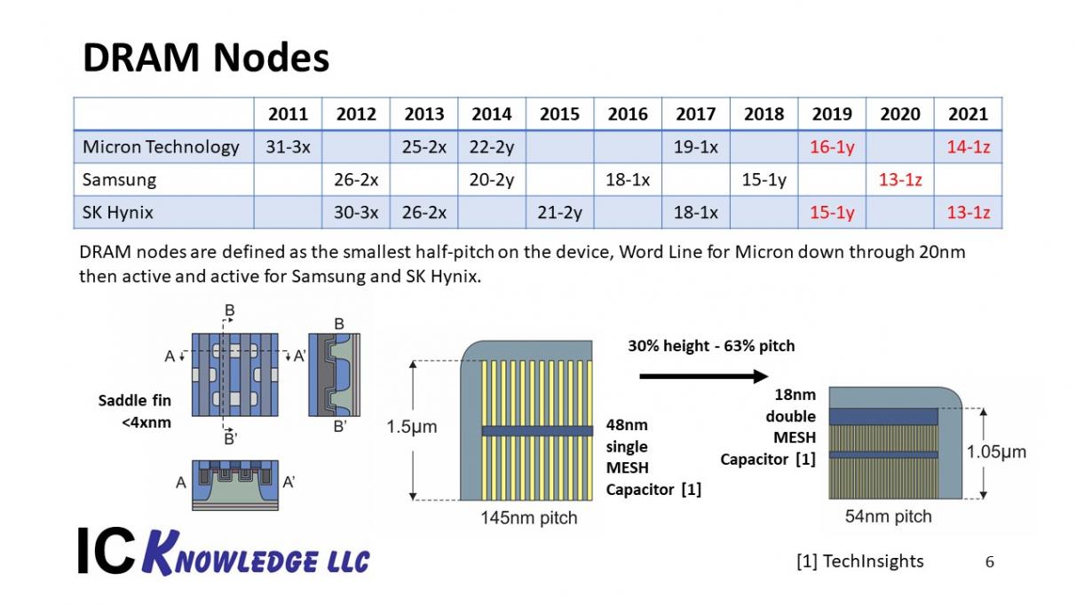
Figure 4. DRAM Nodes
In figure 4 was can see the DRAM nodes by company. In the bottom of the slide as some of the key technical accomplishments. On the bottom left is the Saddle Fin access transistor that is universally used in DRAM today. On the bottom right the capacitor scaling from a 48nm node to and 18nm node are illustrated.
Figure 5 illustrates DRAM capacitor scaling.
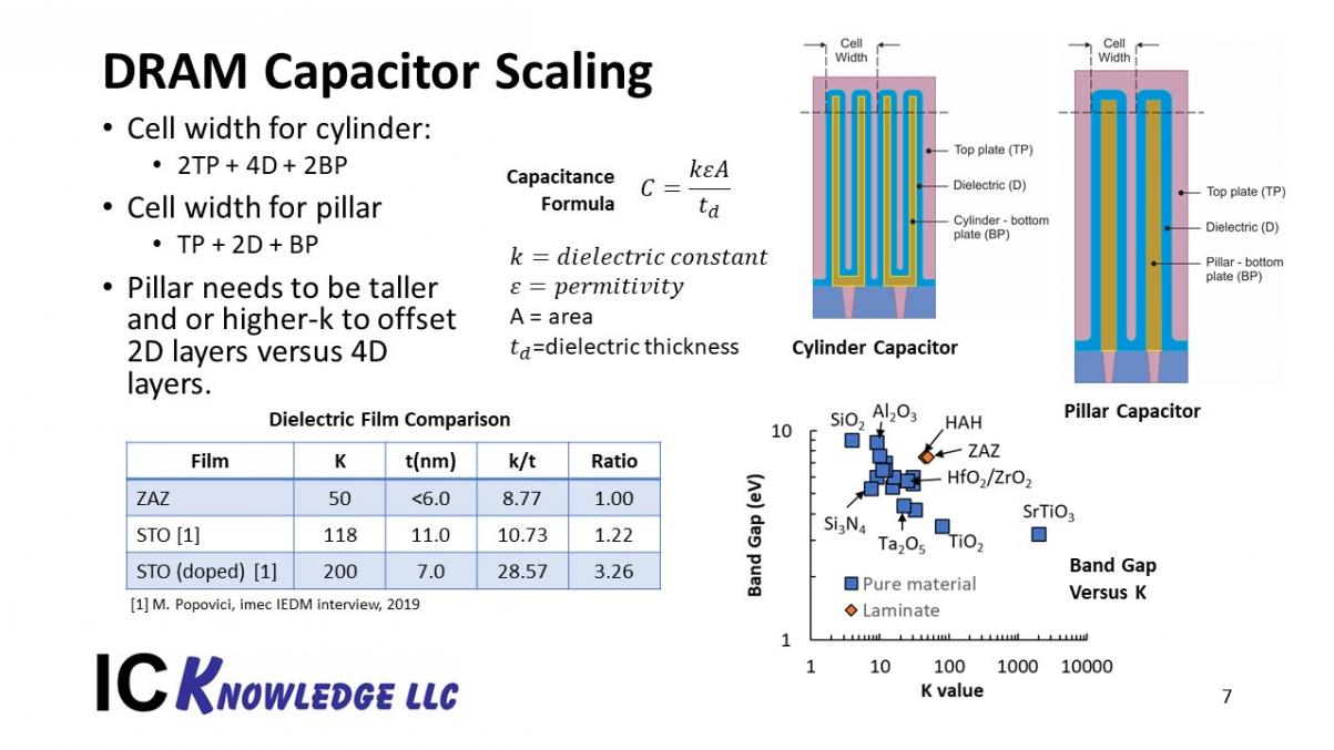
Figure 5. DRAM Capacitor Scaling
A DRAM stores values as a charge or lack of charge on a capacitor. In order to retain the value and sense it reliably, a minimum value of capacitance is required. The capacitance of a capacitor is given by the k value of the film multiplied by a constant and the area of the capacitor divided by the film thickness. Ideally, we want to make capacitors smaller to shrink DRAM but that lowers capacitance. We have used the vertical dimension to increase the 3D area of the capacitors while shrinking the horizontal area, but we are facing mechanical limits on height. The film thickness of the dielectrics is already about as thin as it can be without leaking too much. From the graph in the lower right we can see that as k value increases band gap generally decreases and decreasing band gap increases leakage.
One interesting recent result reported by Imec at IEDM 2019 is a strontium titanate based film with higher k vales that if thick enough can achieve acceptable leakage. Of course making the film thicker lowers capacitance so the figure of merit of a film becomes k/t where t is the thickness for acceptable leakage. The table in the bottom left lists the current zirconium oxide – aluminum oxide – zirconium oxide (ZAZ) film versus the current Imec STO film and a doped STO film Imec believe they can achieve. The figure of merit for the current ZAZ film is 8.77, for the Imec work 10.73, a 1.22x improvement and if Imec can achieve their projected films the figure of merit would 28.57 and a 3.26 improvement. It should be noted that the Imec work is in the early stages, they are experimenting on planar structures and there are patterning challenges for actual use.
Going to a thicker film would require changing the capacitor structure. The current cylinder structures have 2 bottom storage plate thicknesses, 4 dielectric thicknesses and 2 top storage plate thicknesses in each cell. In order to accommodate a thickness dielectric film the cell would need to change to meet the cell size requires. A pillar structures a one top storage plate thickness, 2 dielectric film thicknesses and a bottom storage plate thickness in a call width. This make shrinking the cell easier but by having 2 dielectric thicknesses instead of four you have half the capacitance unless you make the pillar taller. Pillars are mechanically more robust and should be able to be taller but probably not 2x taller. However, if a film can be achieve such as the Imec projected STO (doped) the figure of merit is 3.26 better and even for the same height would increase capacitance.
Figure 6 illustrates some other DRAM scaling issues.
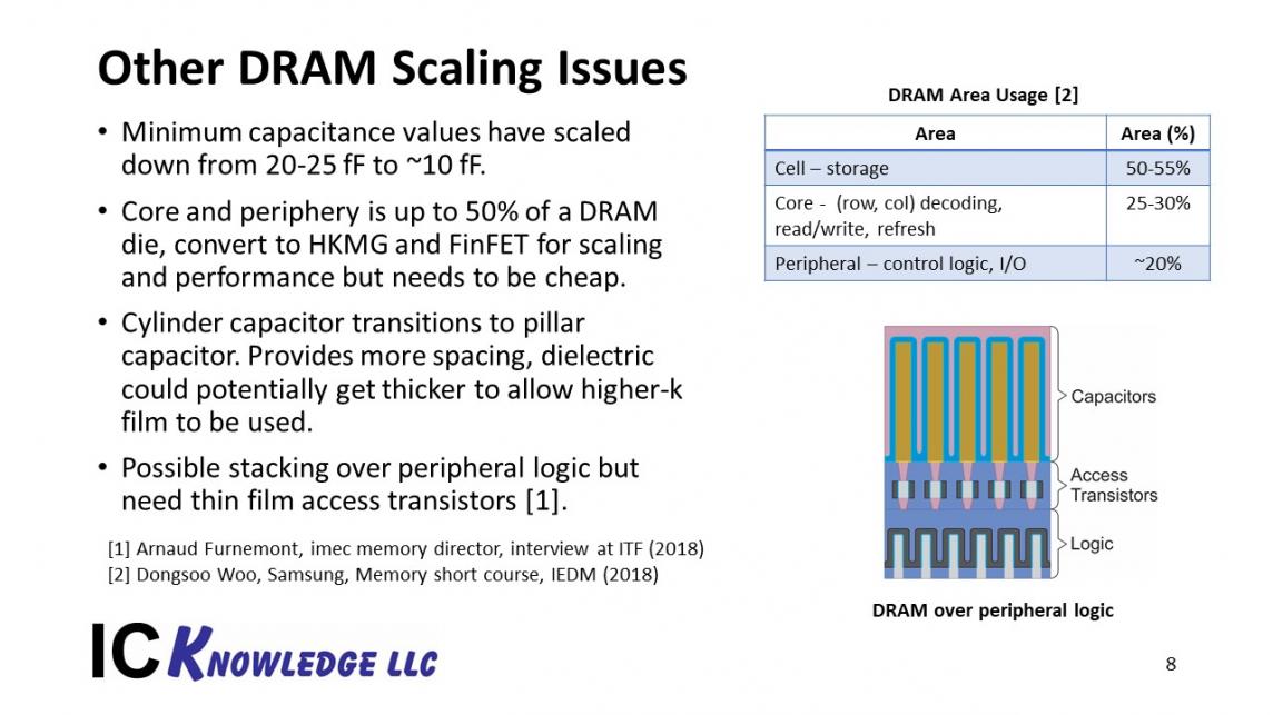
Figure 6. Other DRAM Scaling Issues
Figure 6 summarizes some other DRAM scaling issues, specifically:
- Minimum capacitance values have scaled down from the 20-25fF that was once considered a minimum to around 10fF. This has been achieved by optimizing the drive circuitry and sense amps.
- As the table in the top right shows core and peripheral circuitry makes up roughly 50% of a DRAM die and shrinking these circuits has helped shrink the DRAM die. Eventually these transistors will change over to high-k metal gates (HKMG) and FinFETs but it needs to be done inexpensively.
- As previously discussed cylinder capacitors may change to pillar capacitors to provide more room for the dielectric films.
- If thin film transistors can be developed with low enough leakage stacking DRAM capacitors over access transistor over the logic could be a one-time scaling booster.
Figure 7 illustrates the mask counts for DRAMs.
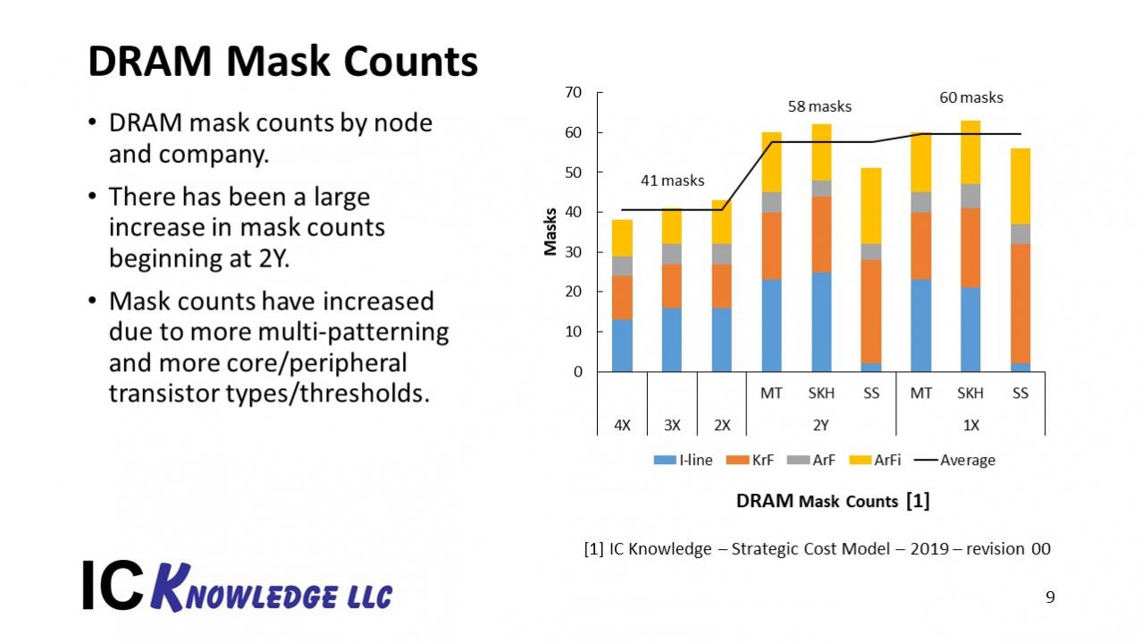
Figure 7. DRAM Mask Counts
The need to optimize the peripheral and core transistor has driven a big increase in transistor counts for multiple transistor types and threshold voltages. This is updated from last years presentation where we under estimated mask counts for 2y and beyond DRAM.
Figure 8 illustrates the bit density trend for DRAM.
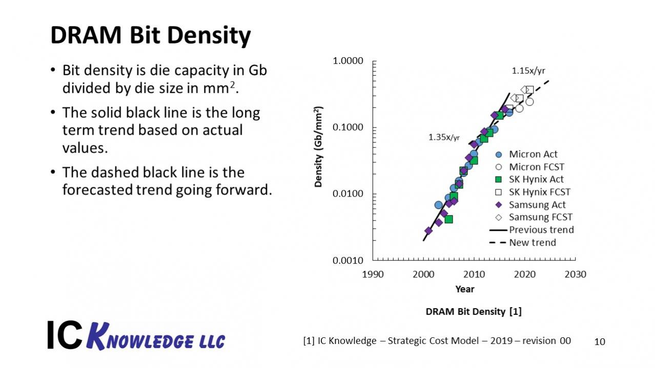
Figure 8. DRAM Bit Density
From figure 8 we can see that up until just after 2010 DRAM bit density was growing by 1.35x/year and then since then bit density growth has slowed to around 1.15x/year.
Logic – High Performance and Internet of Things (IOT)
Leading edge logic has evolved from planar transistors to a split roadmap with FinFET for high performance and things like FDSOI for IOT. Longer term gate-all-around is on the horizon.
Figure 9 illustrates Logic Gate ALL Around (GAA)
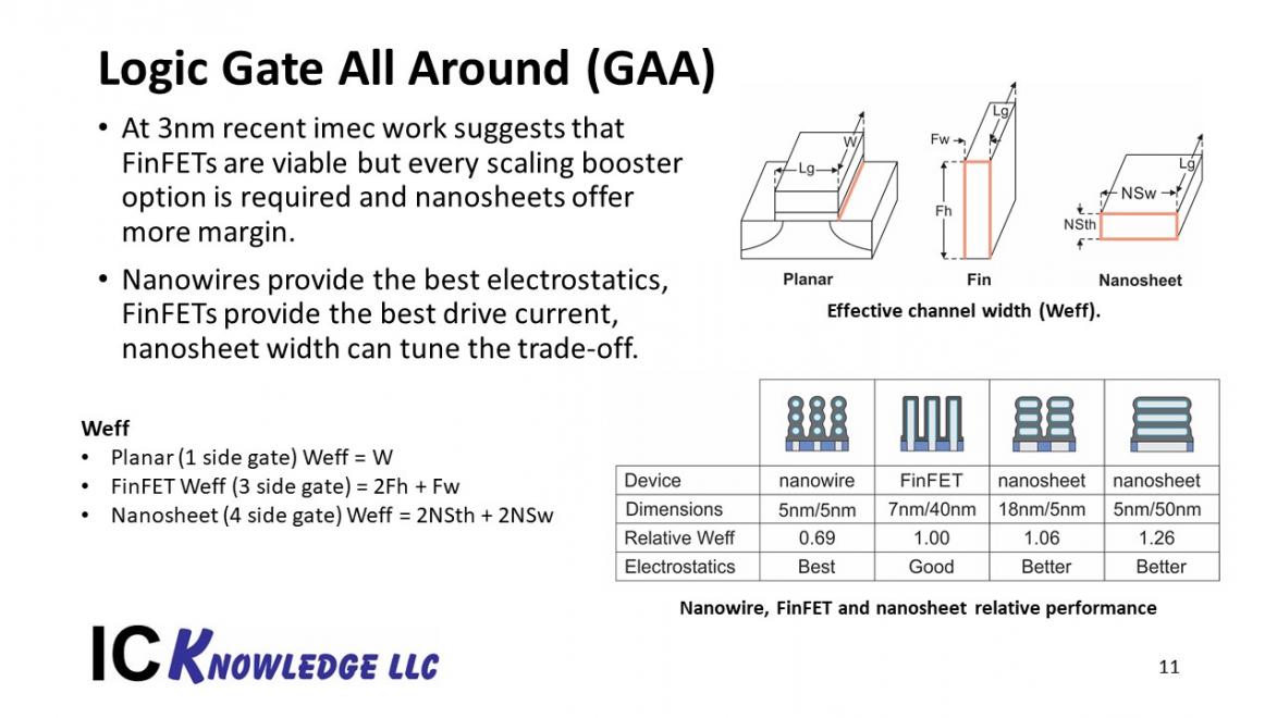
Figure 9. Logic Gate All Around (GAA)
From figure 9 we can see that for planar transistors the effective gate width (Weff) was deifned by the transistor gate width. For FINFETs the Weff depends on the width and 2x the height of the fin and therefore Weff can only be varied in discrete increments. With GAA the Weff is 2x thickness and 2X width. The ability to vary the width can enable variable Weff again and also enable transistor optimization. For example from the lower right we can see that horizontal nano-wire (HNW) have the best electrostatics but less Weff per unit area than a FinFET. With horizontal nano-sheets varying the width can provide more Weff per unti area than a FinFET with better electrostatics although not as good as a HNW.
Figure 10 illustrates a Leading Edge 2D to 3D Logic Roadmap
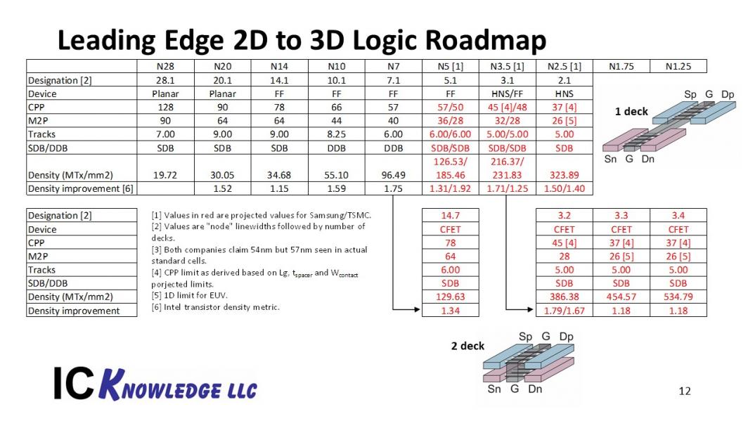
Figure 10. Leading Edge 2D to 3D Logic Roadmap
In figure 10 a roadmap from 2D planar transistors at the 28nm and 20nm nodes to FinFETs and then HNS and eventually stacked 3D CFETs is shown. Down through N7 typical foundry logic dimensions are shown.
For N5 and N3.5 we have specific projections for Samsung and TSMC. At N2.5 we have a generic forecast with both companies converged on HNS.
For 3D we have options beginning with a relaxed 14nm design rule CFET with 7 layers as well as more lithographically aggressive 3.2, 3.3 and 3.4 CFETs with 3nm lithography and 2, 3 and 4 layers. The pictures show an nFET and pFET side by side for a single layer device and then a pFET over and nFET for a 2 layer CFET.
Figure 11 illustrates the mask counts for the various companies and projected out through a 2 layer CFET.
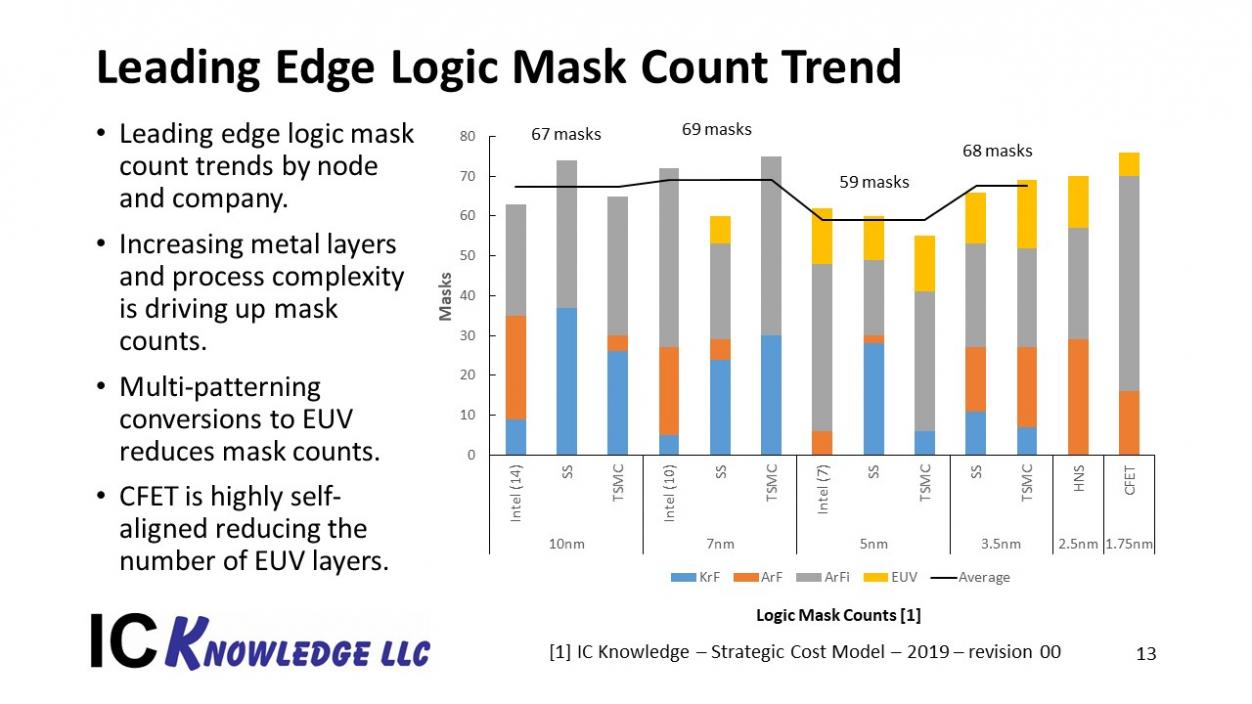
Figure 11. Leading Edge Logic Mask Count Trend
An interesting feature of this graph is how EUV helps to mitigate mask count increases. CFET at a 1.75nm node also helps to control the lithographic difficulty by being highly self-aligned.
Figure 12 presents FDSOI processes for IOT applications.
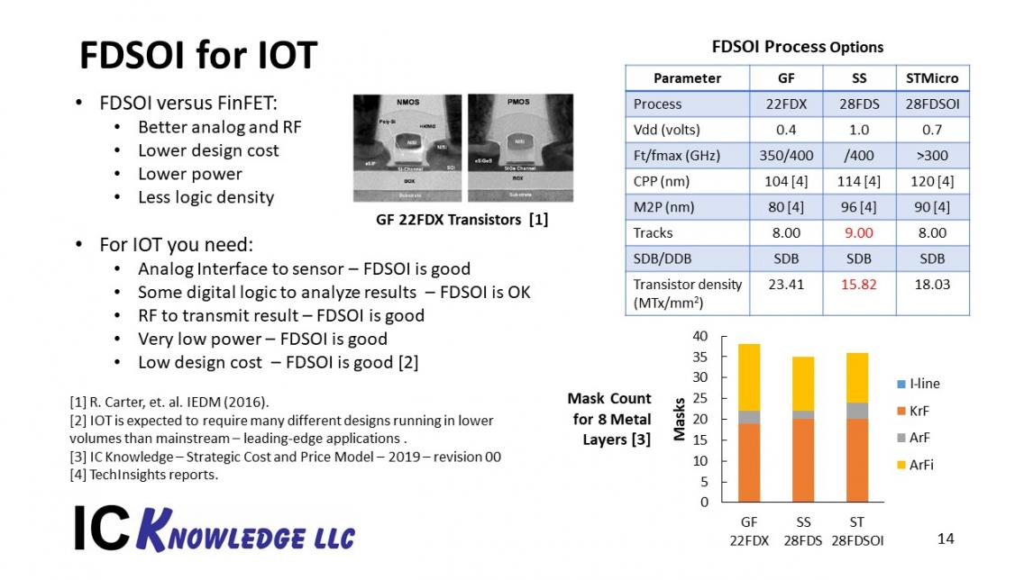
Figure 12. FDSOI for IOT
The requirement for IOT to interface with analog sensors, process the results, store results and transmit them wirelessly is an excellent match for FDSOI processes. Simpler FDSOI processes also can be less expensive to design for and produce relative to FinFETs.
The table on the right side summaries the FDSOI processes from the three leading providers with GLOBALFOUNDRIES showing the densest, lowest power and higher RF performance. The graph on the lower right illustrates the mask counts for the processes. It is interesting to contrast the mask counts in the mid-30s to the FinFET processes with mask counts in the 60s.
Figure 13 illustrates nonvolatile embedded memory options that are being explored or offered by various companies.
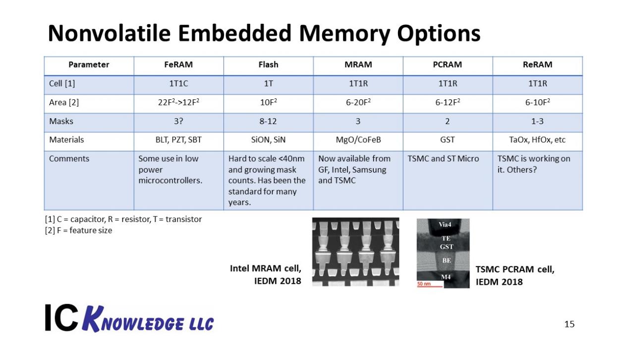
Figure 13. Nonvolatile Embedded Memory Options
In figure 13 five major alternatives for embedded nonvolatile memory are illustrated. Historically Flash ha been widely used and FeRAM has seen some use in low power microcontrollers. Currently MRAM is getting the most attention with all the leading edge foundries and Intel supporting it. PCRAM and ReRAM are getting attention but are not as mature.
Conclusions
NAND has transitioned from 2D lithography driven processing to 3D etch and deposition driven processing. Pitches are relaxed from 2D values and unlikely to get tighter in the future. Mask counts will grow due to string stacking.
DRAM scaling is capacitor limited and facing fundamental physical limits. Scaling is focused on core and periphery improvements with a potential new high-k dielectric on the horizon. Scaling is slowing.
Logic is continuing to scale lithographically but fundamental limits on 2D shrinks are looming. CFETs offer a possible 3D scaling path that could result in relaxed lithographic dimensions analogous to what has happened with 3D NAND. IOT and other applications are driving interest in simpler FDSOI processes and emerging embedded memory.
Acknowledgement
I would like to thank TechInsights for permission to use data from their reports in my presentation.


Comments
20 Replies to “LithoVision 2019 – Semiconductor Technology Trends and their impact on Lithography”
You must register or log in to view/post comments.