







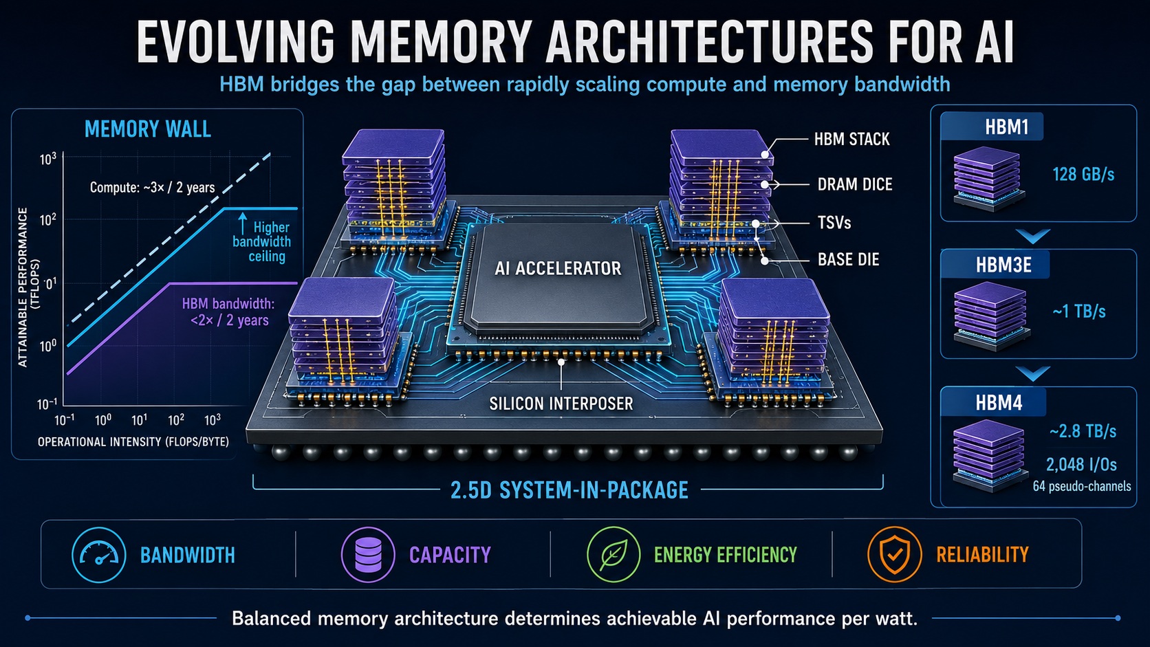
Artificial intelligence performance is increasingly constrained by memory rather than arithmetic throughput. Scaling laws show that model quality improves when parameter count, training data, and compute grow together, but this balance fails when processors cannot obtain operands quickly enough. Contemporary accelerators have expanded floating-point capability at roughly threefold every two years, while high-bandwidth memory bandwidth has advanced at less than twice that rate. The widening gap creates a memory wall: expensive compute units stall, utilization falls, and system-level energy is consumed moving data instead of executing useful operations.
High Bandwidth Memory addresses this imbalance through architectural parallelism and close physical integration. Unlike conventional DDR dual-inline memory modules, HBM places vertically stacked DRAM beside a GPU or accelerator within a system-in-package. Through-silicon vias connect the DRAM layers to a base die, while dense, short interposer wiring connects the base die to the host. This topology supports thousands of relatively low-frequency data connections, achieving very high aggregate throughput without relying exclusively on power-hungry serial signaling.
Generational scaling illustrates the approach. HBM1 provided 1,024 data I/Os and approximately 128 GB/s nominal bandwidth. HBM3E retains 1,024 I/Os but increases signaling rate, channelization, bank count, and stack capacity to reach about 1 TB/s per stack. HBM4 doubles the interface to 2,048 I/Os, expands to 32 channels and 64 pseudo-channels, and targets roughly 2.8 TB/s. Each generation combines faster transfers with finer access granularity and greater density, improving both sustained bandwidth and capacity for model parameters, key-value caches, activations, and training state.
The roofline model explains the performance effect. Arithmetic intensity measures operations performed per byte transferred. Workloads below the sloped bandwidth ceiling are memory-bound; additional compute cannot accelerate them. Increasing HBM bandwidth raises that ceiling, allowing attention, embedding, sparse, and data-movement-heavy kernels to sustain more operations before becoming bandwidth limited. At system scale, eight HBM3 stacks can theoretically supply about 5.3 TB/s, compared with roughly 307 GB/s from an eight-channel DDR5 server configuration. DDR offers much higher capacity, but HBM delivers an order-of-magnitude bandwidth advantage near the accelerator.
This capability carries substantial implementation cost. HBM3E uses far more banks and interface circuitry than DDR5, and its architecture, packaging, and manufacturing requirements consume roughly three times more silicon per delivered capacity. Larger stacks and higher activity also increase heat flux. Coefficient-of-thermal-expansion mismatches among silicon, solder, mold compounds, interposers, and substrates create chip-package interaction risks. Taller stacks complicate heat extraction, power delivery, mechanical integrity, and test coverage. Liquid cooling, improved thermal paths, hybrid bonding, glass substrates, and larger interposer technologies are therefore becoming enabling components rather than optional refinements.
Reliability must scale with bandwidth. Beginning with HBM3, protection operates at two levels: system-visible metadata can support CRC or ECC across each access, while on-die symbol-based Reed-Solomon correction protects internal arrays and transfers. These mechanisms must be coordinated with fault isolation, repair, telemetry, and serviceability so that a single memory defect does not disrupt a large accelerator cluster.
Capacity remains important because models, contexts, and caches increase the working set. Designers must therefore evaluate usable bandwidth, locality, contention, refresh overhead, and fault tolerance together. A nominal interface rate is valuable only when controllers, banks, and software expose enough parallelism to sustain it under realistic access patterns.
Why it Matters: Future memory systems will require co-optimization across DRAM process technology, base-die logic, die-to-die PHYs, interposers, substrates, cooling, power delivery, firmware, and workload scheduling. Advanced base dies may add customized control, data movement, or processing functions, reducing traffic across constrained interfaces. Co-packaged optics can extend bandwidth beyond the package, while fusion and hybrid bonding can increase vertical interconnect density and lower energy per bit. The central design objective is no longer maximum compute alone; it is balanced delivery of bandwidth, capacity, reliability, and energy efficiency. HBM functions as the bridge between rapidly scaling accelerators and the data-intensive behavior of modern AI, making memory architecture a primary determinant of achievable intelligence per watt, per package, and per dollar.
Also Read:
The Twelve-Month Rule Does Not Describe a New Fab
How TSMC Is Wiring the AI Era With Light
Share this post via:



SEMICON West’s Autonomous Fab Vision Needs a Decision-Escalation Design