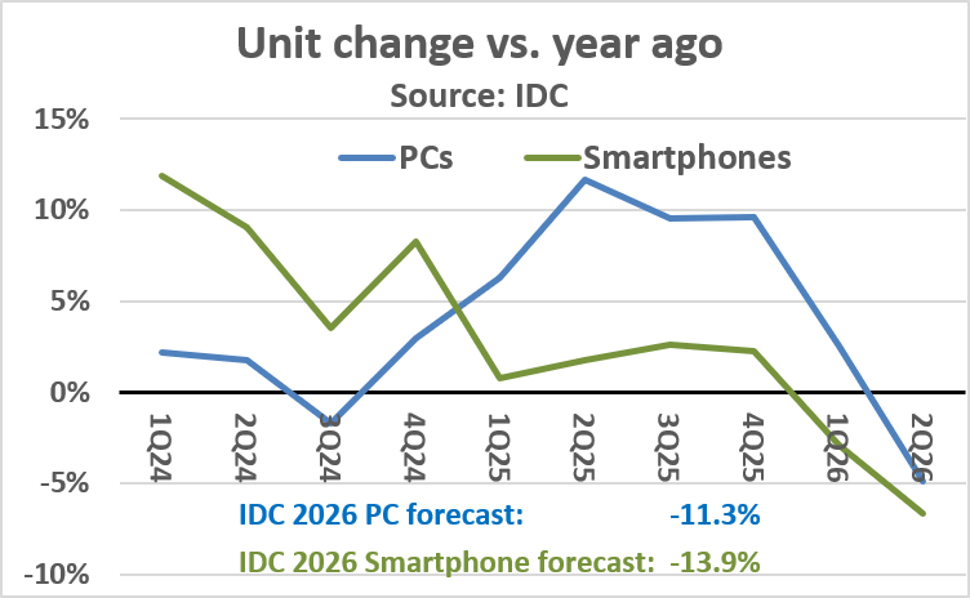
Things just got interesting in the iPhone supply chain with the $1B AAPL Vs QCOM legal action filed this week. For the life of me I could not understand why Apple second sourced the normally QCOM modem in the iPhone 7. It caused quite a stir in the technical community but we could only surmise that it was a price issue on the business side.… Read More
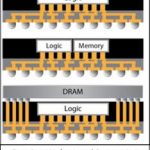
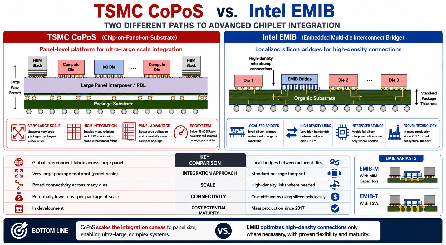 TSMC CoPoS Versus Intel EMIB Semiconductor PackagingTSMC’s CoPoS, generally described as Chip-on-Panel-on-Substrate, and Intel’s…Read More
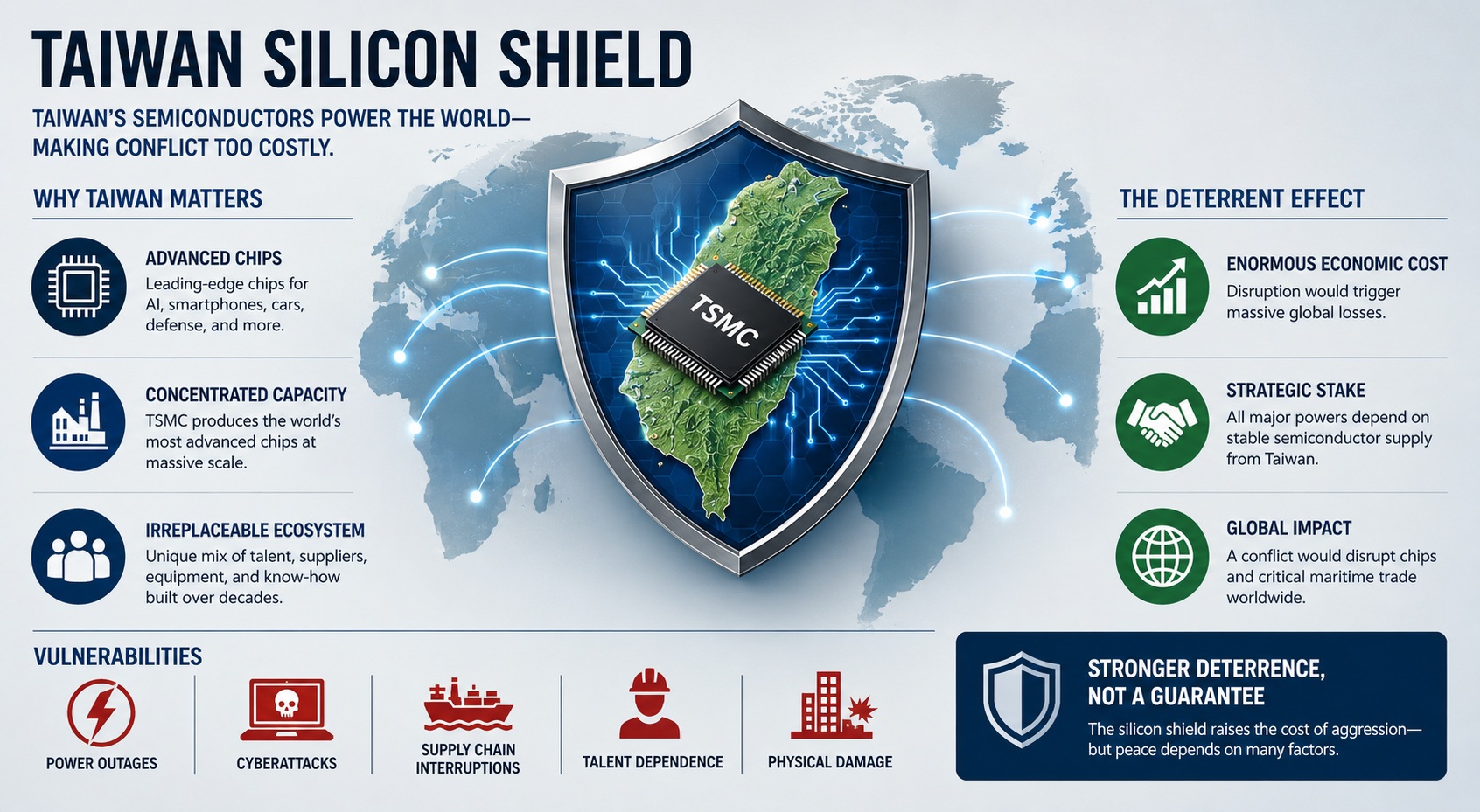 The Silicon Shield Has Never Been Stronger!The “Silicon Shield” describes the idea that Taiwan’s…Read More
 Agentrys Designs a Real Chip with its Multi-Agent WorkforceThe face of EDA is changing. For forty…Read More
 Must-See DAC Panel – Build vs Buy: Who Owns the Intelligence Behind Tomorrow's Chips?This year, DAC will be buzzing about AI…Read More
Power Management Beyond the Edge
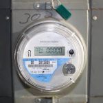
Power in IoT edge devices gets a lot of press around how to make devices last for years on a single battery charge, significantly through “dark silicon” – turning on only briefly to perform some measurement and shoot off a wireless transmission before turning off again. But we tend to forget that the infrastructure to support… Read More
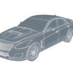
From Tragedy to Triumph for Tesla
Tesla Motors has done it again. Dragged before the investigators of the National Highway Traffic Safety Administration (NHTSA), Tesla was found faultless and its vehicles flawless in connection with the fatal Florida crash last year.… Read More
Mentor Safe Program Rounds Out Automotive Position
Mentor has an especially strong position in the automotive space given their broad span of embedded, SoC, mechanical and thermal and system design tools. Of course, these days demonstrating ISO 26262 compliance is mandatory for semiconductor and systems suppliers, so EDA vendors need to play their part to support those suppliers… Read More
Qorvo and KeySight to Present on Managing Collaboration for Multi-site, Multi-vendor RF Design

Over the last several weeks I’ve been having a lot of discussions with colleagues around IP reuse and design data management. This led me to a discussion with Ranjit Adhikary, Marketing Vice President for ClioSoft.
ClioSoft is best known for their design collaboration software platform called SOS. They also sell an enterprise… Read More
DARPA Flex Logix and TSMC!
When I first saw emerging semiconductor IP company Flex Logix actively involved with TSMC I knew something big was coming and boy was I right. DARPA announced today that an agreement is in place with Flex Logix to develop EFLX eFPGA technology on TSMC 16FFC for use by companies or Government agencies designing chips for the US Government.… Read More
Technology Update With Andrew Faulkner and Jim Lipman of Sidense
Sidense is an interesting company in a very important market segment. Sidense was founded in 2004 and their 1T-OTP memory macros are now used in hundreds of chips from 180nm to 16nm for code storage, secure encryption keys, analog and sensor trimming and calibration, ID tags, and chip and processor configuration.
If you are designing… Read More
Another Interesting Thing From TSMC!
As I mentioned in my previous post, the TSMC investor call this month was very interesting and Morris Chang was in fine form during the Q&A. As a semiconductor professional I think some of the questions are ridiculous but maybe they have value to the financial people. This one question from Randy, who I think is very astute, is … Read More
TCAD Simulation of Organic Optoelectronic Devices
In my office there are plenty of LED displays for me to look at throughout the day: three 24″ displays from Viewsonic, a 15″ display from Apple, an iPad, a Samsung Galaxy Note 4, a Nexus tablet, a Garmin 520 bike computer, and a temperature display. LED and OLED displays are ubiquitous in all sorts of consumer electronics,… Read More
Fan-Out Wafer Level Processing Gets Boost from Mentor TSMC Collaboration
I caught up with John Ferguson of Mentor Graphics this week to learn more about a recent announcement that TSMC has extended its collaboration with Mentor in the area of Fan-Out Wafer Level Processing (FOWLP).
In March of last year Mentor and TSMC announced that they were collaborating on a design and verification flow for TSMC’s… Read More
Enhancing Multi-Domain System Simulation with FMI Co-Simulation