I think by now a lot has been said about the necessity of multi-patterning at advanced technology nodes with extremely low feature size such as 20nm, because lithography using 193nm wavelength of light makes printing and manufacturing of semiconductor design very difficult. The multi-patterning is a novel semiconductor manufacturing technique which realizes a layout by decomposing it into 2 or more parts and then separate mask exposure (with double or more pitch for extra resolution) for each part which are later recombined to get the original layout. FinFETs on the other hand are new 3D transistors (with gate wrapped around the channel) which can provide extreme power-performance-area advantage to high density, high performance and multi-functionality SoCs. While these technologies are proven in processing and manufacturing, EDA P&R tools need significant revamping to accommodate these for their use in designs at mass scale. How to make provisions for multi-patterning and FinFETs during layout design and verification?

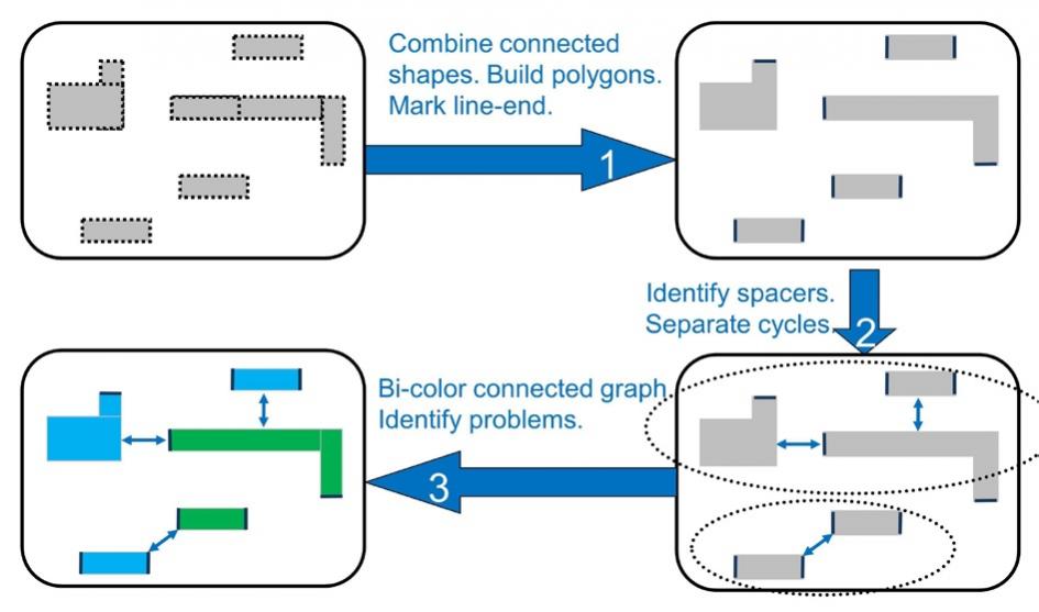
The layout is decomposed by a concept called ‘coloring’, where adjacent shapes in a layer are assigned different colors such that same colors are not at violating distance. It’s a complex problem to solve; intelligent algorithms need to be applied to solve a dense layout which can have millions of shapes in complex forms. Above is an example of cycles (a graph formation between layout shapes and spacers), where an odd cycle is in coloring violation due to two nodes being in same color and even cycle is clean. Many a times, sensitive design structures such as memories, clocks, analog matched pairs etc. need pre-coloring (anchoring) which puts constraint in coloring other shapes, thus making the layout more prone to non-resolvable coloring violation. Then there are techniques used at foundry level to remove errors such as self-conflicting layout, rounding, misalignment etc. which need to have their provisions in P&R tools as well.
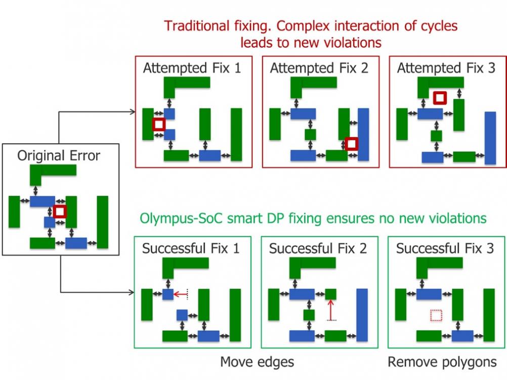
Clearly, the multi-patterning rules significantly increase the complexity and computation for routers which are already burdened with ever increasing DRC rules; run-time and QoR are at stake. The router needs to natively understand colors, and detect, fix and verify any multi-patterning violation which can have local or global impact (fixing one violation can create new violations elsewhere), unlike DRC fixes which are local in nature.
Similarly FinFETs pose another set of challenges such as voltage-threshold aware spacing, implant layer rules, fin grid alignment, source-drain abutment rules etc. on placement, floorplanning and optimization engines. An interesting point to note is that FinFETs are implemented at process nodes below 20nm at which multi-patterning becomes a must, thus increasing the challenges for P&R tools to handle large set of complex rules. The interactions between FinFET restrictions and multi-patterning rules in the layout need to be considered at all stages of the back-end flow including placement, routing and optimization.

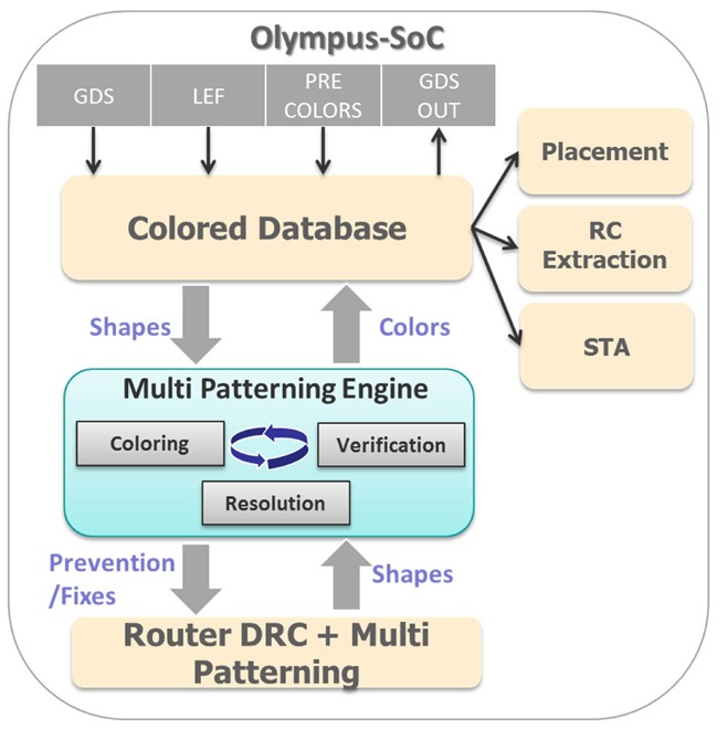
I’m impressed with Mentor’sOlympus-SoC P&R system that provides a comprehensive platform for effectively dealing with all these challenges at advanced process nodes with its unique database capable of handling multiple masks. The system supports complete DRC and multi-patterning rules for leading foundries and has tight integration with Calibre to insure sign-off clean physical verification with minimal design interaction. The router is smart enough to color the layout natively, efficiently resolve conflicts and fix violations at local and global level for fast multi-patterning closure.

An effort to prevent multi-patterning conflicts takes place very early in the flow, at the time of coloring and decomposition. The router automatically extracts several patterns such as end-of-line in dense configuration forming small odd cycles and that in sparse configuration leading to long odd cycles, and tries to avoid such configurations and others in order to gain faster convergence.

The prevention of conflicts leads to a reduced set of violations to be fixed. It’s essential to clean up as many DRC violations as possible before proceeding with multi-pattern fixing. The majority of the multi-patterning violations are fixed in small, local search and repair windows in a global context. The multi-pattern fixing handles both nested and interdependent cycles, and minimizes design perturbation. The DFM optimization is multi-patterning aware and does not introduce any new cycle.
The placement engine in Olympus-SoC is FinFET and multi-patterning aware. By default, it supports the fin grid for both standard cells and macros, because the placement grid is a multiple of the fin grid. The detailed placer considers implant spacing requirements for minimum width and area and supports continuous diffusion and poly-over-diffusion edge abutment rules. Intelligent filler insertion ensures implant and OD shape matching. The different combinations of standard cells are taken into account and the cells are either spaced apart or flipped in their orientations to ensure that no violations are created.
The built-in color aware parasitic extraction engine accurately models the 3D parasitic requirements of FinFETs and also handles capacitance variation due to mask shift which can impact timing and design performance. The extractor can correctly model the effects of mask shift and write out triplet SPEF (nominal, best, and worst case values) which can be read by MCMM timing engine to correctly time the design.

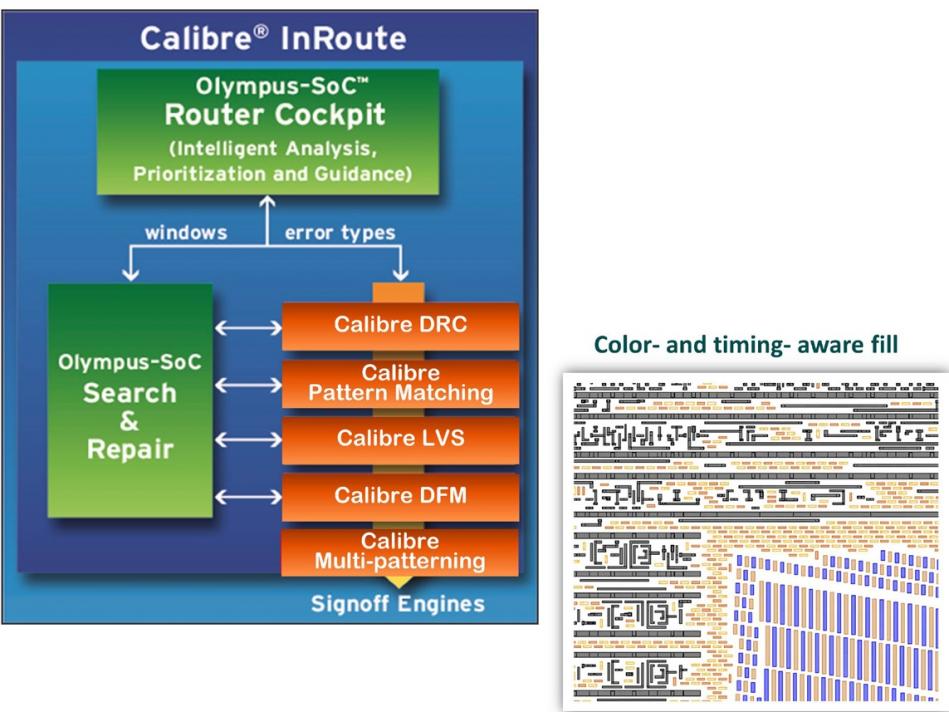
The Calibre InRoute addresses the advanced requirements of intelligent color and timing aware metal fill and true sign-off analysis against all DRC, DFM and multi-patterning violations. The Olympus-SoC platform provides native SVRF support including metal fill and double-patterning decks. Uniformity of metal fill density across different masks is maintained. By using Calibre InRoute, a faster time-to-market can be realized due to significant speed up in manufacturing sign-off process along with high QoR.
The Olympus-SoC P&R system offers a flexible and powerful architecture to address multi-patterning and FinFET requirements and can concurrently analyze and optimize the various design metrics including timing, power and signal integrity across all modes and corners (MCMM). The optimization engine performs dynamic density recovery, white space optimization and area management throughout the flow for best design utilization. A more detailed description along with reference literature on multi-patterning, Olympus-SoC and Calibre InRoute can be found in a whitepaperposted at Mentor website.

More Articles by Pawan Fangaria…..
lang: en_US
Share this post via:


Comments
0 Replies to “FinFET & Multi-patterning Need Special P&R Handling”
You must register or log in to view/post comments.