You are currently viewing SemiWiki as a guest which gives you limited access to the site. To view blog comments and experience other SemiWiki features you must be a registered member. Registration is fast, simple, and absolutely free so please,
join our community today!
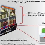
The way we are seeing technology progression these days is unprecedented. It’s just about six months ago, I had written about the intense collaboration between ANSYSand TSMCon the 16nm FinFET based design flow and TSMC certifying ANSYS tools for TSMC 16nm FF+ technology and also conferring ANSYS with “Partner of the Year” award.… Read More
Metal fill requirements for inductors are now a fact of life. Fill has long been seen as detrimental to device performance due to parasitic capacitance. The necessity of fill arises from the need to ensure planarization of dielectric layers by using chemical mechanical polishing. Without adequate fill, areas of the chip can suffer… Read More
I think by now a lot has been said about the necessity of multi-patterning at advanced technology nodes with extremely low feature size such as 20nm, because lithography using 193nm wavelength of light makes printing and manufacturing of semiconductor design very difficult. The multi-patterning is a novel semiconductor manufacturing… Read More