You are currently viewing SemiWiki as a guest which gives you limited access to the site. To view blog comments and experience other SemiWiki features you must be a registered member. Registration is fast, simple, and absolutely free so please,
join our community today!
One of my favorite EDA disruptions is the Siemens acquisition of Mentor, pure genius. Joe Sawicki now runs the Mentor IC EDA business for Siemens so we will be seeing him at more conferences and events than ever before. Joe did a very nice keynote at the recent U2U conference that I would like to talk about before we head to the 56thDAC… Read More
I’m at the 2015 imec technology forum (ITF) in Brussels the next few days. One of the presentations today was by Peter Wennink, the CEO of ASML. The thing that most interested me in his presentation is what the status of EUV is today. ASML is the only company developing EUV steppers so what they think is important. On the other … Read More
On the Cadence booth at DAC, Lars Liebmann of IBM presented on the challenges of 10nm. As he put it, how the lithography folks are keeping things very interesting for the EDA tool development engineers. Although 14nm/16nm hasn’t yet ramped into HVM, the advanced work for tools and IP has all moved to 10nm. Although Lars gave… Read More
Place & route in the 16/14nm era requires a new approach since it is significantly more complex. Of course, every process generation is more complex than the one before and the designs are bigger. But modern processes have new problems. The two biggest changes are FinFETs and double patterning.
FinFETs, as I assume you know,… Read More
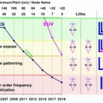
All the details of how we will build semiconductors going forward depend on whether we have EUV in our arsenal or not. Imec is very close to this since they work closely with ASML (who are about an hour and half’s drive away just outside Eindhoven in the Netherlands). At the imec technology symposium we were given a quick summary… Read More
To wrap up Semicon West, let’s go back to Monday and the imec presentations. In fact, An Steegen’s presentation titled The Semiconductor Roadmap. She covered a lot of ground, but some of her slides contain a wealth of information. Let’s look at the options for 10nm, 7nm and a little 5nm, what imec call N10, N7 and… Read More
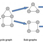
I think by now a lot has been said about the necessity of multi-patterning at advanced technology nodes with extremely low feature size such as 20nm, because lithography using 193nm wavelength of light makes printing and manufacturing of semiconductor design very difficult. The multi-patterning is a novel semiconductor manufacturing… Read More
As you can’t have failed to notice by now, 28nm is the last process node that does not require double patterning. At 20nm and below, at least some layers require double patterning. The tightest spacing is typically not the transistors but the local interconnect and, sometimes, metal 1.
In the litho world they call double patterning… Read More
I’ve been quite impressed that modern ICs use a lithography process with 193nm light sources to resolve final feature sizes at 20nm and smaller dimensions. We’ve been blogging about Double Patterning Technology (DPT) some 45 times in the past few years that enable 20nm fabrication, so one big question for me is, “How… Read More
At major EDA events, CEDA (the IEEE council on EDA, I guess you already know what that bit stands for) hosts a lunch and presentation for attendees and others. This week was ICCAD and the speaker was Lars Liebmann of IBM on The Escalating Design Impact of Resolution-Challenged Lithography. Lars decided to give us a whirlwind tour … Read More