You are currently viewing SemiWiki as a guest which gives you limited access to the site. To view blog comments and experience other SemiWiki features you must be a registered member. Registration is fast, simple, and absolutely free so please,
join our community today!
I am at ARM TechCon today. One interesting presentation was made jointly between Samsung, Cadence and ARM themselves about developing physical libraries (ARM), a tool flow (Cadence) and test chips (Samsung). It was titled Samsung ARM and Cadence collaborate on the silicon-proven world first 14-nm FinFET Cortex-A7 ARM CPU and… Read More
Diagnosing Double Patterning Violationsby Beth Martin on 10-28-2013 at 5:16 pmCategories: EDA, Siemens EDA
I’ll bet you’ve read a bunch of stuff about double patterning, and you’re probably hoping that the design tools will make all your double patterning issues just go away. Well, the truth is that the foundries and EDA vendors have worked really hard to make that true.
However, for some critical portions of your design, there … Read More
Engineers are always looking to improve the efficiency of how they work, but don’t want to sacrifice accuracy in the process. This is true in the world of semiconductor process development, where traditional build-and-test cycles are both time and resource intensive. But what if there was a way to do certain steps in a ‘virtual’… Read More
It is beginning to look as if 28nm transistors, which are the cheapest per million gates compared to any earlier process such as 45nm, may also be the cheapest per million gates compared to any later process such as 20nm.
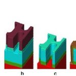
What we know so far: FinFET seems to be difficult technology because of the 3D structure and so the novel manufacturing… Read More
I think by now all of us know, or have heard about 20nm process node, its PPA (Power, Performance, Area) advantages and challenges (complexity of high design size and density, heterogeneity, variability, stress, lithography complexities, LDEs and so on). I’m not going to get into the details of these challenges, but will ponder… Read More
Back in May, William Holt, EVP of technology and manufacturing at Intel gave a presentation to analysts entitled Advancing Moore’s Law, Imperatives and Opportunity. A pdf of the presentation is available here. I just saw it for the first time today and I’m not sure how to get my head around it. It starts off with a lot … Read More
Round #1 was here.
In the EUV corner were Stefan Wurm of Sematech (working on mask issues mostly) and Skip Miller of ASML who are the only company making EUV steppers (and light sources, they acquired Cymer).
You may know that the biggest issue in EUV is getting the source brightness to have high enough energy that an EUV stepper has … Read More
If you want to know the state of play in lithography, there is no better place than the special session on lithography at Semicon West. This year was no exception. The session was given the punchy title Still a tale of 2 paths: multi-patterning lithography at 20nm and below: EUVL source and infrastructure progress.
In the blue corner… Read More
Every process node these days has a new “gotcha” that designers need to be aware of. In some ways this has always been the case but the changes used to be gradual. But now each process node has something discontinuously different. At 20nm the big change is double patterning. At 14/16nm it is FinFET.
Rahul Deokar and John… Read More
Chasing DP Rabbitsby SStalnaker on 04-15-2013 at 4:00 pmCategories: EDA, Siemens EDA
“Now, here, you see, it takes all the running you can do, to keep in the same place. If you want to get somewhere else, you must run at least twice as fast as that!”
—Lewis Carroll, Through the Looking Glass
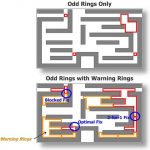
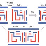
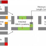
The use of stitching can greatly reduce the number of double patterning (DP) decomposition violations that a designer has to resolve.… Read More