I’ve been quite impressed that modern ICs use a lithography process with 193nm light sources to resolve final feature sizes at 20nm and smaller dimensions. We’ve been blogging about Double Patterning Technology (DPT) some 45 times in the past few years that enable 20nm fabrication, so one big question for me is, “How does this effect my design and verification flow?”
David Abercrombie of Mentor Graphics authored a 12 page white paper, “Mastering the Magic of Multi-Patterning” and it answers that question about the impact on design and verification flows with multi-patterning.

David Abercrombie
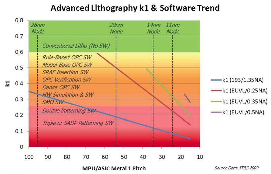
The International Technology Roadmap for Semiconductors (ITRS) uses a value called K1to define process-related factors, and the following chart shows K1 plotted versus the Metal 1 pitch size and what software is required during the IC layout flow:
Multi-Patterning (MP) Techniques
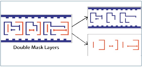
Starting at the 20nm node several IC layers must use DPT to decompose one drawn layer into two mask layers:
- Active MOS device
- Contact
- Via
- Lower metal layers
These layers at 20nm are just too dense to be printed in a single exposure, so they are split into two less-dense layers where the foundry adds extra exposure steps called Litho-Etch-Litho-Etch (LELE) pitch-splitting:
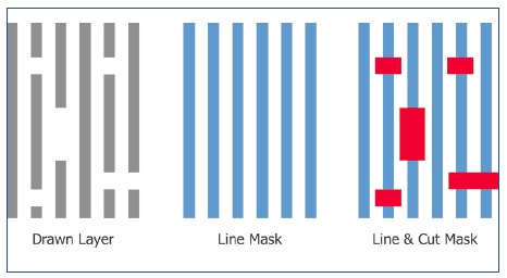
A restrictive design rule at 20nm is for the gate layer to be oriented only in one direction, and the drawn layer is then automatically split into a line mask and cut mask:
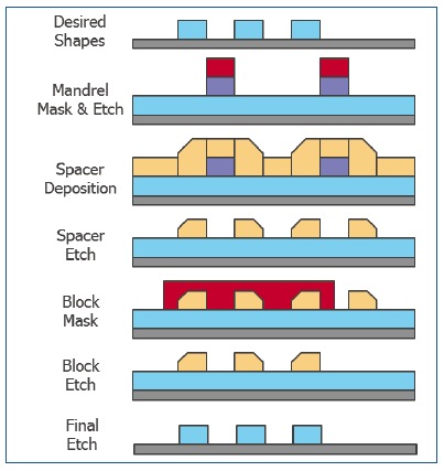
FinFETS in the 16 and 14nm nodes require a technique known as Spacer-Assisted Double Patterning (SADP). The IC designer does their layout of FinFETs and the foundry creates these extra Mandrel and Block masks.
At 10nm DP doesn’t work any more, so a Triple Patterning (TP) technique has to be used, where a single layout layer gets decomposed into three separate masks as shown by three colors:
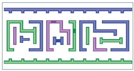
MP Color Control
There are four approaches to creating the two mask layers in a DP design flow:
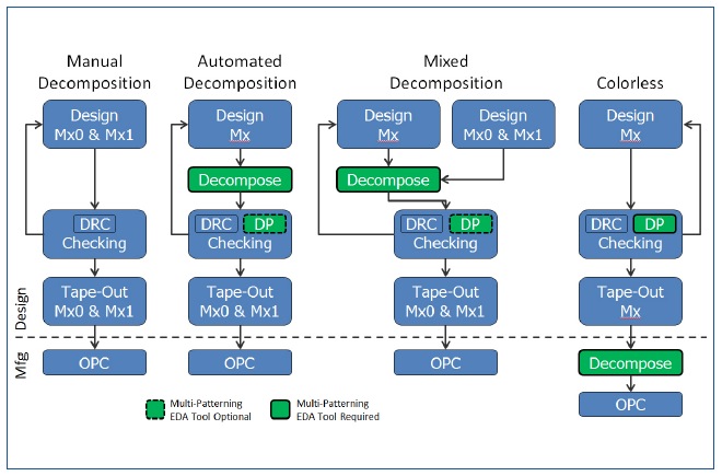
The manual decomposition flow requires the most manual labor and debug time, so it’s not really practical.
With automated decomposition you draw just a single layer and then use software like Calibre Multi-Patterning to create the two masks and check for MP correctness.
In the mixed decomposition flow you would be combining previously decomposed layout IP with new layout.
The fourth approach is Colorless, where you just do layout in the traditional sense and rely upon the foundry to run MP checks and do the decomposition as a service.
Critical Nets
With MP comes the side effect of misalignment between decomposed layers, and that changes the parasitic resistance and capacitance values, which in turn effect the timing on critical nets. You can decide to take more control over the decomposition process in order to minimize the side effects of coloring. Anchoring lets you assign a shape to a particular mask, which then limits the automated coloring to fewer choices. Seeding marks part of a polygon to set the color for the remainder of the shape.
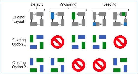
MP Layout Debug
With MP there are new layout checks for compliance, similar to traditional DRC error checking:
- Opposite mask spacing
- Self-conflict violation
- Anchor self-conflict
- Odd cycle violation (red)
- Anchor/Seed path violation (dark purple)
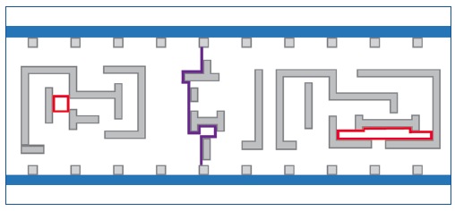
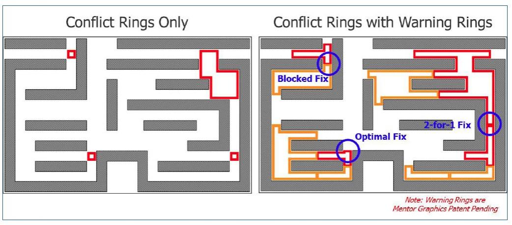
Fixing these violations is trickier than just moving one polygon, because the change could then introduce new MP errors. With the Calibre MP tool you get some relief by seeing both a conflict ring and warning ring, so that you can concentrate your attention on fixing the spacings that are not included in a warning ring first:
Odd Cycle Violations
To fix an odd cycle violation you could move the polygons farther apart, which increases the layout size or introduces a new error. The second approach is to cut a polygon and make it have two colors and stitch the colors together:
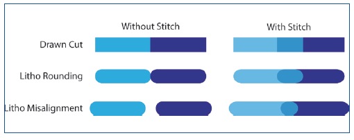
Check with your foundry to see if they support the cut/stitch methodology.
MP Layout and Parasitics
Coupling capacitance between adjacent layers is impacted by the use of DP and TP masks as they are misaligned:
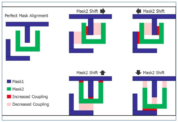
Calculating the capacitance values can be either extraction-based (common corners-based) or analysis-based (statistical analysis with sensitivities to spacing). For extraction-based the foundries supply info on the dielectric constant change as a function of polygon width and spacing to other polygons. This adds more corners for analysis, which just takes more analysis time.
The simulation-based approach uses Monte Carlo analysis for analog designs, or statistical static timing analysis for digital designs.
Cell Placement
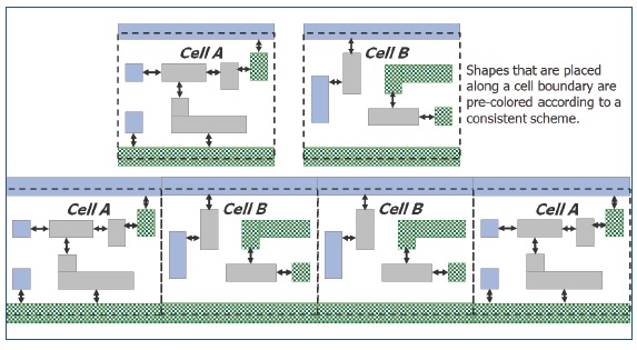
Placing cells at fixed heights along rows can introduce MP errors like odd cycle:
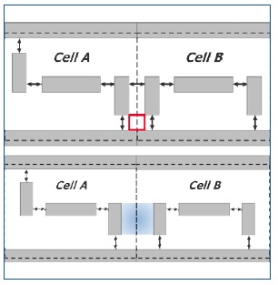
One approach to avoid this odd cycle error is to design each cell with anchoring on polygons next to the cell borders with a consistent scheme:
Routing Between Cells
Your MP routing strategy depends on the cell strategy, and one approach is to constrain the cell pin coloring with pre-coloring or anchoring.
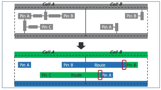
Odd cycle violations can be found and fixed automatically, however at the expense of longer run times. Mentor has added MP prevention in it’s P&R tool called Olympus-SoC. You can even run Calibre MP inside of Olympus with an integration called Calibre iRoute.
Conclusion
You can design, layout and verify an SoC using 20nm, 16nm or even 10nm with the help of MP technology, a new methodology, advise from your foundry and newer MP-aware EDA tools. Yes, it’s more work, but that’s the price to exploit the latest foundry technologies.
Read the complete White Paper here.
lang: en_US
Share this post via:


Comments
There are no comments yet.
You must register or log in to view/post comments.