You are currently viewing SemiWiki as a guest which gives you limited access to the site. To view blog comments and experience other SemiWiki features you must be a registered member. Registration is fast, simple, and absolutely free so please,
join our community today!
The SPIE Advanced Lithography Conference is the semiconductor industries premier conference on lithography. The 2023 conference was held the week of February 27th and at the conference Applied Materials announced their Sculpta® pattern shaping tool. Last week I had an opportunity to interview Steven Sherman the Managing … Read More
At the ISS Conference in January, An Steegen EVP of Semiconductor Technology & Systems at imec gave a talk entitled “Patterning Options for Advanced Technology Nodes”. I was present for her talk and had the opportunity to have a follow up interview with An.… Read More
On Tuesday morning at SEMICON I had the opportunity to sit down with Harry Levinson, Sr. Director of Technology Research and Sr. Fellow at Global Foundries and Michael Lercel, Director of Strategic Marketing at ASML to discuss the state of lithography.
I opened the discussion with a question about how we are going to address lithography… Read More
More than 500 designers (562) have responded to a survey made in 2015 by Synopsys. Answering to the question “What is the fastest clock speed of your design?” 56% have mentioned a clock higher than 500 MHz (and still 40% higher than 1 GHz). If you compare with the results obtained 10 years ago, the largest proportion of answers was for… Read More
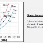
The way we are seeing technology progression these days is unprecedented. It’s just about six months ago, I had written about the intense collaboration between ANSYSand TSMCon the 16nm FinFET based design flow and TSMC certifying ANSYS tools for TSMC 16nm FF+ technology and also conferring ANSYS with “Partner of the Year” award.… Read More
Some of Intel’s technology posts make some pretty specific statements and I have seen a number of posts where people seem to have misinterpreted what Intel was actually saying.
Multi Patterning
I have seen a lot of confusion on this one with some people saying Intel didn’t use multi patterning at 22nm and others saying Intel used … Read More
I think by now a lot has been said about the necessity of multi-patterning at advanced technology nodes with extremely low feature size such as 20nm, because lithography using 193nm wavelength of light makes printing and manufacturing of semiconductor design very difficult. The multi-patterning is a novel semiconductor manufacturing… Read More
Last week I attended the SPIE Advanced Technology Conference. There were a lot of interesting papers and as is always the case at these conferences, there was a lot of interesting things to learn from talking to other attendees on the conference floor.
The first interesting information from the conference floor was that 450mm is… Read More