
More than 500 designers (562) have responded to a survey made in 2015 by Synopsys. Answering to the question “What is the fastest clock speed of your design?” 56% have mentioned a clock higher than 500 MHz (and still 40% higher than 1 GHz). If you compare with the results obtained 10 years ago, the largest proportion of answers was for clock ranging between 100 MHz to 300 MHz.
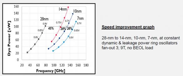
That means that Moore’s law has been extremely effective during the last ten years, and also that for a high proportion of designs, speed improvement is a real need. These designs are the natural candidates to target FinFET technologies. From the graph below, you see that moving from 28nm (bulk) to 14nm FF can provide 45% faster frequency, at constant dynamic & leakage power, each step below, 10nm and 7nm, providing another 20% improvement.

Foundries like TSMC, Samsung or GlobalFoundries are in charge of the technology development and companies like Synopsys have to provide EDA tools and design enablement, foundation, memories and mixed-signal IP. Reading the presentation made by Navraj Nandra during the Silicon Valley SNUG last March will give you a very good understanding of the challenges linked with nodes like 7nm FF, and the way Synopsys has overcome these challenges to design standard cell libraries, memories and interface (mixed-signal) IP. These foundation IP had to be optimized for Power, Performance and Area for 14nm FF, 10nm FF and 7nm FF, just like it was done for now mature nodes, 65nm, 40nm or 28nm.
If you take the example of the RC associated with BEOL, the value per um is moving from 5 E-15 for 14nm FF, to 10.5 E-15 for 10nm FF and up to 21.6 E-15 for 7nm FF, or doubling for every node. Another challenge is the metal pitch, requiring double patterning below 40 nm. Moreover, you can’t just scale down the 10nm standard cell library to target 7nm, but you have to lower the fin count, called “Fin Depopulation”, to lower dynamic power while preserving speed and reducing standard cell density. You even can get an additional 20% speed improvement by using specialized cells & assist circuits and managing electrostatic control.
As well, you can’t just re-use memory compiler, as you have to create new embedded self-test and repair to address new 7nm defects, like process variation induced (fin height, fin pitch or lithography issues), systemic and random faults. Moreover, managing low resistance and parasitic line capacitance are becoming critical at 7 nm, remember that RC value is doubling at every node…
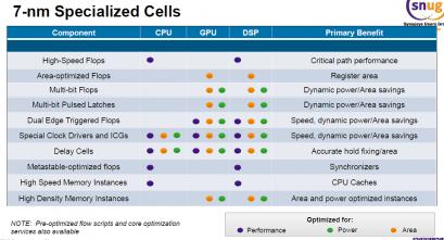
The above table gives you an overview of the many specialized cells developed by Synopsys for 7 nm, optimized for a combination of Performance, Power and Area to target CPU, GPU or DSP. The effort is worth to do, as, after decreasing both the metal pitch and the gate pitch, you benefit from the scaling factor, improving Area, exhibiting much higher Performance (speed improvement graph) and lower Power consumption: PPA has been optimized and this is the first consequence of Moore’s law.
Complexes, multicore SoC designed in 7 nm will certainly integrate CPUs, or GPUs or DSPs, and probably a combination of all these cores. When integrated in the system, such a SoC will interface with DRAM based on DDR3 or DDR4, or LPDDR3, 4 protocol, communicate thanks to USB 3.1 or PCI Express 4.0, to name a few. Before developing such complex IP, a vendor has to evaluate the market size (the TAM) to calculate the ROI and make the decision to invest in heavy development. From this well-known graphic built by Synopsys, we can evaluate the number of cumulated design starts per node, since the technology introduction. After zoom in the graphic, we come to about 200 design starts for 16/14 FF and 50 for 10 and 7nm. This sanity check is very positive, if the IP vendor can afford development cost and expect reasonable market share (usually, Synopsys enjoys in the 40-60% market share for interface IP), the ROI should be great.
From the presentation made at SNUG, we understand that developing for 7 nm interface IP like DDR4, PCIe 4.0 or USB 3.1 type C, to name a few, require satisfying more stringent requirements than for previous bulk-based technologies. The layout effort doubled, due to Restricted Design Rules (RDR) and multi-patterning. To address reliability and process variability issues for digital IP, RAS features has to be implemented for PCIe 4.0 or DDR4, through stronger data protection like parity or ECC in conjunction with protocol defined mechanism to detect and correct errors in the data path and RAMs. He will have to use event counters and statistics to monitor system availability and to leverage error injection and silicon debug capabilities to diagnose issues and validate system recovery. The result will be 30% improved area and power compared to previous FinFET nodes.
You can find many blogs talking about the end of Moore’s law, at least as Moore’s law used to be: faster and cheaper transistor when going down by one node. The introduction of FinFET based technologies is a way to continue Moore’s law by packing more transistors and cores in a SoC with higher performance and lower power. If you asking if there is a market for these FinFET nodes, the 200 design starts in 14/16 nm FinFET is the answer. The chip makers or OEM targeting fin FET need EDA tools, foundation IP (standard cell library and memories) and interface IP portfolio and Synopsys has demonstrated that they offer these down to 7 nm.
From Eric Esteve from IPNEST
You will also benefit from this video here.
Share this post via:


Comments
There are no comments yet.
You must register or log in to view/post comments.