You are currently viewing SemiWiki as a guest which gives you limited access to the site. To view blog comments and experience other SemiWiki features you must be a registered member. Registration is fast, simple, and absolutely free so please,
join our community today!
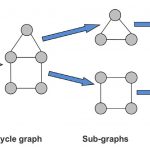
I think by now a lot has been said about the necessity of multi-patterning at advanced technology nodes with extremely low feature size such as 20nm, because lithography using 193nm wavelength of light makes printing and manufacturing of semiconductor design very difficult. The multi-patterning is a novel semiconductor manufacturing… Read More
With multiple functionalities added into a single chip, be it a SoC or an ASIC, maintaining low power consumption has become critical for any design. Various techniques at the technology as well as design level are employed to accomplish the low power target. These include thinner oxides in transistors, different sections of … Read More
Introduction
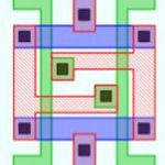
IC designs go through a layout process and then a verification of that layout to determine if the layout layer width and spacing rules conform to a set of manufacturing design rules. Adhering to the layout rules will ensure that your chip has acceptable yields.
At the 28nm node a typical DRC (Design Rule Check) deck will… Read More